Low Temperature Selective Si and Si-Based Alloy Epitaxy For Advanced Transistor Applications
- PDF / 888,434 Bytes
- 6 Pages / 612 x 792 pts (letter) Page_size
- 72 Downloads / 252 Views
0913-D04-05
Low Temperature Selective Si and Si-Based Alloy Epitaxy for Advanced Transistor Applications Yihwan Kim, Ali Zojaji, Zhiyuan Ye, Andrew Lam, Nicholas Dalida, Errol Sanchez, and Satheesh Kuppurao Epi KPU, Front End Product Group, Applied Materials, 974 E. Arques Ave., M/S 81288, Sunnyvale, California, 94085
ABSTRACT We have developed low temperature selective Si and Si-based alloy (SiGe and Si:C) epitaxy processes for advanced transistor fabrications. By lowering epitaxy process temperature (≤ 700 oC), we have demonstrated elevated source/drain formation on ultra-thin (< 50 Å) body SOI transistors without Si agglomeration, smooth morphology of selective SiGe epitaxy with high [Ge] (>30 %) and [B] (>2E20 cm-3) concentrations, and selective Si:C epitaxy with high substitutional C concentration (>1 %). Also, we have increased growth rate of low temperature selective epitaxy processes by optimizing process parameters by adapting non-conventional deposition method.
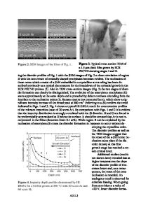
INTRODUCTION Conventional scaling metal-oxide-semiconductor (MOS) transistors for increasing device speed faces limitations beyond 65 nm technology node. In order to boost the device performance further, selective Si and Si-based alloy epitaxy processes have been recognized as solutions. Selective Si, SiGe, and Si:C epitaxy can be used for so-called elevated and recessed source/drain (S/D) applications. The elevated S/D decreases source/drain sheet resistance and also plays role as a buffer layer to protect S/D from etch damage during contact hole formation [1]. Also, elevated S/D is required to form fully depleted SOI transistors [2]. In recessed S/D application, an area below the level of the gate dielectric is etched and filled with SiGe or Si:C epitaxy depending on PMOS or NMOS transistor. This application enables one to fabricate faster transistors without shrinking the gate length by enhancing carrier mobility via uniaxial compressive or tensile strain of the transistor channel [3-6]. Need for low temperature epitaxy process results from two aspects: One is thermal budget of advanced transistor fabrication. At lower epitaxy temperatures, low growth rates are concern. The other is from a material property aspect. Strain relaxation of SiGe epitaxy and high substitutional carbon concentration in Si:C epitaxy are good examples of why epitaxy temperature should be kept low. Because the solid solubility of substitutional carbon in silicon is only ~1017 cm-3, carbon atoms at concentrations higher than this easily incorporate into interstitial sites or precipitate as β-SiC, resulting in no strain in the epilayer. Therefore, in order to achieve high substitutional carbon concentration (Csub ≥ 1%), non-equilibrium epitaxial growth conditions such as low temperature are required. It is well known that strained SiGe epitaxy with higher [Ge] is more easily relaxed at a given condition.
We have developed low temperature selective Si, SiGe, and Si:C epitaxy processes for advanced transistor applications and will review result of each epitaxy process. EX
Data Loading...