Measurement of Electroplated Copper Overburden for Advanced Process Development and Control
- PDF / 172,395 Bytes
- 6 Pages / 612 x 792 pts (letter) Page_size
- 15 Downloads / 252 Views
K4.10.1
Measurement of Electroplated Copper Overburden for Advanced Process Development and Control Joshua Tower1, Alexei Maznev1, Michael Gostein1, and Koichi Otsubo2 1 Philips Advanced Metrology Systems, Inc., 12 Michigan Drive, Natick, MA 01760 USA 2 Philips Advanced Metrology Systems, Inc., Kohnan, Minato-ku, Tokyo 108-8507 Japan
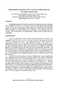
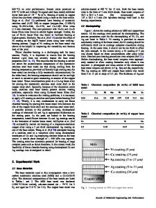
ABSTRACT We used a non-contact metrology system based on laser-induced surface acoustic waves to evaluate the thickness uniformity of electroplated copper. Several wafers were prepared using different plating conditions that affect the copper overburden thickness and uniformity. Measurements of overburden were made on a variety of pattern features including trench arrays of several pattern densities, solid bond pads, and the surrounding field area. In general, the overburden was found to be thicker above the arrays of narrow linewidth, as compared to the surrounding field. However, the magnitude of this “mounding” effect is dependent on the plating process, pattern density, and position on the wafer. For example, as the accelerator in the plating solution increases, the mounding on a 50% density line array varies from zero to 5000 Angstroms. Under all plating conditions used, the mounding was found to be progressively higher as the pattern density of the array increases (in the range of 20% to 50% copper). The solid pads were found to have conformal filling, in all cases. It was also found that the overburden in the field area is reduced as the adjacent mounding increases, presumably because the reactant in the plating bath becomes depleted in the vicinity of the high overburden regions above the arrays. INTRODUCTION The wafer-level and die-level uniformity of the copper electroplating process has a direct effect on the final post-CMP thickness of copper interconnect lines used in advanced integrated circuits [1]. Control of the plating process involves a complex balance between the chemical properties of the plating bath, the variable parameters of the plating machine, and the characteristics of the incoming wafer. The challenge is to minimize the amount of copper overburden that is plated onto the wafer while maintaining a uniform fill for features of highly varying density. Unfortunately, post-plating thickness can depend greatly on the local feature geometry, with some process conditions resulting in excess deposition above narrow-linewidth structures [2]. The resultant mounding above such structures can lead to uniformity problems at the subsequent CMP step. Mounding can be reduced by modifications to the plating process. However, optimizing these process conditions and keeping them under control requires metrology for copper thickness over a variety of structures on the wafer. Obviously, it is not possible to approach this problem using blanket monitor wafers with large-area measurement techniques, e.g. four-point probe, because the electroplated copper thickness depends critically on the linewidth and pattern density
K4.10.2
in the local area of the wafer. Therefore, techniq
Data Loading...