Measurement of Thin Film Mechanical Properties by Microbeam Bending
- PDF / 1,427,098 Bytes
- 6 Pages / 417.6 x 639 pts Page_size
- 67 Downloads / 436 Views
Abstract An improved microbeam bending technique has been developed for the study of mechanical properties of thin films on substrates. This testing method utilizes a triangular beam geometry and improved micromachining techniques compared to previously used methods. The technique permits the stress-strain law for a metal film on a substrate to be determined. Single crystal Si beams and bi-layer Si/Al beams of lengths 25-100 pgm have been fabricated and tested. The beams are deflected with a nanoindenter, which accurately imposes a load on the beam and measures the corresponding displacement. For the bi-layer beams, a simple numerical model utilizing a Ramburg-Osgood constitutive law the film has been developed to determine the stress-strain behavior of the Al film.
Introduction There is a continuing need for the development of new techniques to study the mechanical properties of microelectronic thin films. Currently, techniques such as nanoindentation, wafer curvature, and bulge testing are used to measure thin film mechanical properties [ 1.2]. While indentation has proven to be a simple and easy-to-use technique, it fails to provide the fundamental data (yield strength, strain hardening rate) needed for the characterization and modeling of thin film structures. Wafer curvature also provides useful information about the elastic and plastic behavior of thin films on substrates, but large temperature changes are required for these experiments and only global averaged properties of the film can be determined. Bulge testing has also produced encouraging results. However, complex processing and testing techniques make it difficult to easily and accurately measure the basic mechanical
properties. Therefore, in an effort to devise a simple method for studying the mechanical properties of thin films on substrates, a microbeam bending technique has been developed. The
method is similar to previous work done on microbeam bending [3-5], except that triangular shaped silicon microbeams are used. These triangular beams have the advantage that the entire film on the top surface of the beams is subjected to a uniform state of strain when the beams are deflected, unlike the standard rectangular geometry where the bending is concentrated at the support. Rectangular and triangular beams have been fabricated by micromachining and deflected using the nanoindenter. The sample geometry coupled with the high resolution of the nanoindenter allows this technique to have high strain resolution.
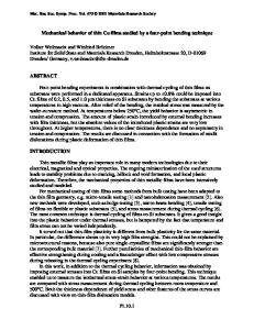
Theory The advantage of the triangular beam is the constant moment per unit width acting in the beam during deflection. As shown in Fig. 1,the bending moment is defined as the product of the load, P and the lever arm, (L-x). Using similar triangles, the moment per unit width can be expressed as: M M1 P(L - X) P(L - X)L PL . .. W,,(L-X) (1) W -..W W, .-constant 0
231 Mat. Res. Soc. Symp. Proc. Vol. 563 ©1999 Materials Research Society
/0z I
L
Fig. 1.Top View Schematic of Triangular Beam This constant moment per unit width results in a const
Data Loading...