Mechanical Property Measurement of Interconnect Materials by Magnetostrictive Sensors
- PDF / 4,987,355 Bytes
- 6 Pages / 612 x 792 pts (letter) Page_size
- 87 Downloads / 410 Views
0968-V04-07
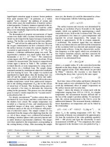
Mechanical Property Measurement of Interconnect Materials by Magnetostrictive Sensors Cai Liang, Leslie Mathison, and Barton C. Prorok Auburn University, Auburn, AL, 36849-5341 ABSTRACT This paper reports on the measurement of elastic modulus for some electronic thin film materials used in electronic interconnects by a magnetostrictive sensor. Thin film materials of Au, Sn, In and Au-rich lead free solder (AuSn) were sputter deposited onto well defined strips of MetglasTM. This material possesses magnetostrictive properties whereby it deforms when subjected by a magnetic field and generates a magnetic field when deformed. The MetglasTM strip is driven to resonance via a modulated magnetic field generated by a coil. The elastic modulus of the above materials was determined by measuring the resonant frequency of the sensors before and after film deposition and using the frequency shift, two analytical approaches were employed to extract values. The as sputtered films were examined by X-ray Diffraction (XRD) and Scanning Election Microscope (SEM) to characterize their microstructures. The elastic modulus of Au films was determined by employing two mathematical methodologies that resulted in values of 71.2GPa and 75.9GPa, which exhibit less than 5% divergence. Errors in the different measuring methodologies are discussed. Moreover, elastic modulus values of solder materials of AuSn (80/20 wt%), tin and indium films, which were also measured in their as deposited forms, will be discussed. This method represents a potentially new, non-destructive method to determine critical material properties of as deposited materials. INTRODUCTION Solder materials have been widely employed in electronics interconnection and assembly for a long time. Indium and AuSn (80/20 wt%) solders, in particular, are often applied in the assembly of optical fiber and components. A Au-rich, AuSn eutectic solder for example, is the ideal choice for passive assembly photonics devices [1], not only because of its excellent creep and fatigue resistance and self alignment, but also the fact that AuSn solder can be reflowed without using the flux process [2]. Moreover, AuSn and Indium solders are often used for hermetical packaging for optical device and MEMS[3]. In addition, Pb-based solder materials are banned in many countries due to environmental contamination issues. High temperature, lead free AuSn (80/20 wt %) eutectic solder then becomes one of the most important alternatives for high temperature power device packaging and assembly. The mechanical properties of film materials employed in interconnection and packaging are critical to successful function of the device. Many techniques[4-6] available for measuring thin film material properties require additional fabrication steps to fashion the test structures. These steps may alter the properties of the film material and they are not very cost/time effective. Nanoindentation is simple approach but i influenced by the substrate and the depth of indentation self. All of the techniques emp
Data Loading...