Microstructural characterization of Al 98.5wt. % Si 1.0wt. % Cu 0.5wt. % on chemical-vapor-deposited W
- PDF / 2,234,497 Bytes
- 9 Pages / 612 x 828 pts Page_size
- 68 Downloads / 274 Views
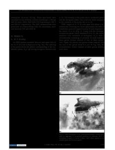
The microstructural and morphological properties of thin (6000 A) Al98.5wt.%Sii.owt.%Cuo.5wt.% films on chemical-vapor-deposited tungsten-coated substrates have been characterized as functions of substrate temperature during deposition and a postdeposition sinter. Scanning electron and transmission electron microscopic investigations show these properties can be categorized with respect to the substrate temperature during deposition. The Al98.5wt.%Si1.owt.%Cuo.5wt.% films deposited on substrates heated at temperatures =S200 °C are rough and are comprised of rounded grains. For deposition on substrates heated at =£300 °C, the films are smooth. Large voids and small precipitates (presumably Al2Cu) are present in the films deposited at 400 °C. The films retain their as-deposited texture during a 450 °C sinter. Precipitates and evidence of W interactions occur in the sintered films deposited on the lower temperature substrates. In addition, the shapes of thermal hillocks and mesa-like protrusions that form during the sintering process are influenced by the films' as-deposited morphologies.
I. INTRODUCTION The demand and complexity of metal interconnects used in ultra-large-scale integrated (ULSI) circuits have increased inversely with the downscaling of their dimensions. The metal interconnects must carry higher current densities and resist corrosion and electromigration while maintaining a low total resistance. Pure Al is attractive as an interconnect because of its low resistivity (2.7 ^til-cm) and easiness to etch. However, it is prone to electromigration for the current densities used in ULSI circuits. Its electromigration resistance can be improved by adding small amounts (~1%) of Cu impurities,1 increasing its grain size,2"5 and maximizing the percentage of the film having the (111) orientation.4"6 Optimizing the amount of Cu in the films is difficult because the Cu segregates in the form of Al2Cu precipitates7"10 during film deposition. A low-temperature (350 °C-450 °C) sinter allows the Cu to redistribute itself along grain boundaries10'11 which, by being pinned, are less prone to electromigration. This sinter has an added benefit of increasing the Al grain size12 which also increases the Al electromigration resistance. The drawback of the sinter step is that micron-sized hillocks form during the sintering process13"15 and interfere with the patterning
a)
Present address: Department of Materials Science and Engineering, Massachusetts Institute of Technology, Cambridge, Massachusetts 02139. J. Mater. Res., Vol. 8, No. 5, May 1993
http://journals.cambridge.org
Downloaded: 15 Mar 2015
process. For this reason the patterning and etch processes must be done prior to the sinter step. Unfortunately, the Al2Cu precipitates present in the film create Al-Al 2 Cu galvanic cells that are susceptible to corrosion during a solvent strip of the photoresist.1617 This corrosion is understood to initiate between the precipitates at the surface of the patterned Al films which then works its way into the bulk of the film. Ex
Data Loading...