Microstructuring of Silica and Polymethylmethacrylate Glasses by Femtosecond Irradiation for MEMS Applications
- PDF / 652,010 Bytes
- 6 Pages / 612 x 792 pts (letter) Page_size
- 71 Downloads / 334 Views
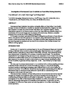
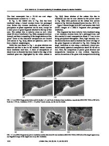
Microstructuring of Silica and Polymethylmethacrylate Glasses by Femtosecond Irradiation for MEMS Applications Saulius Juodkazis, Kazuhiko Yamasaki, Andrius Marcinkevičius, Vygantas Mizeikis, Shigeki Matsuo, Hiroaki Misawa, Thomas Lippert1 Tokushima University, 2-1 Minamijosanjima, Tokushima 770-8506, JAPAN 1 Paul Scherrer Institut, CH-5232 Villigen PSI, SWITZERLAND ABSTRACT We report the fabrication of complex 3D microstructures in silica and polymethylmethacrylate glass by a combination of femtosecond laser microfabrication and chemical wet etching techniques. It is demonstrated that fabrication of interconnected network of channels having lengths of about 200 µm, and diameters as small as 10 µm is possible due to the enhanced etching selectivity (typically 20 - 60) in the laser-irradiated regions. Thus, it becomes feasible to form 3D micro-fluidic and photonic crystal structures in transparent glass-like materials using this approach. In addition, preliminary results on microstructuring of rubber are presented. INTRODUCTION Ever increasing need for miniaturization of various mechanical, optical and electrical devices creates demand to increase the spatial resolution of currently available microfabrication techniques. As far as pulsed lasers are involved in the microfabrication, this demand is transformed into the requirement for lower wavelength and shorter duration pulses. For a fixed laser wavelength, lateral resolution of the microfabrication can not be increased infinitely without compromising the axial resolution [1]. Thus, shorter laser wavelengths, possibly expanding to XUV and X-ray regions will be needed in order to scale down the minimum feature size. In the most foreseeable future eximer lasers are a likely choice , e.g., KrF laser (λ = 248 nm) is already used commercially for lithography with 130 nm resolution, also ArF and and F2 lasers emitting at 193 nm and 157 nm are available. It is necessary to stress here, that similar, albeit slightly longer wavelengths are also achievable with widely popular femtosecond solid state laser systems (e.g., Ti:Saphire ) by higher harmonics generation [2]. In fact, use of such systems has proven indispensable in pushing the spatial resolution of the microfabrication beyond the diffractive limit [3,4]. In this work we demonstrate the capabilities of femtosecond laser microfabrication, which may be further enhanced by combining it with wet chemical etching. Although such approach does not guarantee very high spatial resolution, it enables one to obtain high aspect ratio channel-like microstructures, highly demanded in photonic and microfluidic applications. We report the fabrication of such prototype microstructues in silica and polymethylmethacrylate (PMMA) glasses. EXPERIMENTAL DETAILS The microstructuring experiments were carried out using τp = 150 fs, λ = 800 nm (or 400 nm) pulses of a Ti:Sapphire laser. Laser irradiation was focused inside the samples by a high numerical aperture microscope objective lenses with NA = 0.8-1.35 to the depth of 5-150 µm B5.25.1
(
Data Loading...