Silica Glasses
- PDF / 748,686 Bytes
- 6 Pages / 604.8 x 806.4 pts Page_size
- 30 Downloads / 386 Views
e s t r e n g t h ( — 150 kpsi), and high chemical durability. In a d d i t i o n , bulk forms of silica continue to find application in lenses, p r i s m s , w i n d o w s , a n d lowcoefficient-of-thermal-expansion reflective optics; thin silica films are common components of the highly reflective and antireflective surface coatings which are laid d o w n on reflective a n d t r a n s m i s s i v e optics, respectively. Finally, the use of silicon dioxide as quartz crystal oscillators is familiar to everyone who owns an electronic wrist watch. It is a significant fact that virtually all applications of Si0 2 but the one last mentioned employ an amorphous form of the material. Amorphous silicon dioxide (aSi0 2 ) can be produced in a wide variety of ways. Conventional melting of natural quartz crystals usually comes to mind first, but thermal oxidation of silicon is now familiar from MOS technology. However, the highest purity bulk fused silicas are m a n u f a c t u r e d by flame h y d r o l y s i s or plasma oxidation of silicon tetrachloride to form micron-sized soot or porous boules which then may be sintered in various atmospheres for drying or removing trace i m p u r i t i e s before final d e n s i f i c a t i o n . Doped silicas for fiber optics are produced
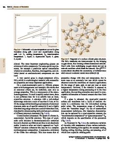
Wavelength (yim) 0.15
12
11
10
9
8
0.2
0.3
0.4 0.5
0.7 -1
0.8 1
0.9 1.0 1 1-
2.0 —i
3.0 5.0 10 1—n—rr
7 Photon Energy
(eV)
Figure 1. Optical attentuation spectra of pure fused silica (including radiationinduced defects) and of unirradiated germanium-doped silica optical fibers. Hollow horizontal arrows indicate the effective ranges of various measurement techniques. Sources of the original data are cited in Reference 2. PAGE 20, MRS BULLETIN, JUNE 16/AUGUST 15, 1987
from the chlorides by chemical vapor deposition, while an alternative way of growing oxide films on silicon is by anodization. Thin a-Si0 2 films may be deposited in vacuo by thermal or electron-beam evaporation or ion-assisted sputtering. Buried a-Si0 2 layers in silicon are fabricated by ion implantation. Sol-gel silicas, long a research curiosity, now seem to be moving out of the laboratory and toward commercialization. Perhaps the most common sol-gel process involves hydration of various alkoxides of silicon in organic solvents, followed by heating stages to remove water and organics. However, gel silicas can also be produced from aqueous slurries of silica soots. Structure of a-Si0 2 Given the great technological importance of a-Si0 2 , it is not at all surprising that considerable basic research has been d e v o t e d to d e t e r m i n i n g its s t r u c t u r e . Indeed, the ability to produce amorphous forms of silica in so many different ways suggests that a-Si0 2 might have more than one identifiable structure. So, what are the structures of amorphous silicon dioxide and how can they be determined? It is best to preface answers to these questions with a disclaimer: It is impossible to deduce the structure of a glass from any experiment. Because amorphous solids
Data Loading...