Modeling and Real-Time Process Monitoring of Organometallic Chemical Vapor Deposition of III-V Phosphides and Nitrides a
- PDF / 2,679,530 Bytes
- 12 Pages / 417.6 x 639 pts Page_size
- 60 Downloads / 209 Views
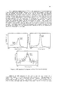
In this paper we discuss the modeling and real-time optical process monitoring of organometallic chemical vapor deposition (OMCVD) at pressures p < 0.1 Pa and p > 105 Pa, respectively. In the low-pressure regime we focus onto monitoring of chemical beam epitaxy (CBE) by p-polarized reflectance spectroscopy (PRS). For reasons described below, at high pressure, PRS must be replaced by other methods, such as, principal angle spectroscopy (PAS) and internal transmission spectroscopy (ITS). Since CBE operates at ultra-high vacuum (UHV) background pressure, it provides access to ultra-high vacuum surface analysis tools. Ballistic transport of source vapor molecules to the surface of a heated substrate assures that all chemical reactions preceding and succeeding incorporation of constituent atoms into growth sites occur on the surface. CBE thus is uniquely suited for investigations of surface decomposition of organometallic and hydride source vapors. In contrast, at higher pressures the increasing rate of molecular collisions, and thermal coupling of the gas phase to the hot substrate, moves the decomposition of source vapor molecules with increasing pressure increasingly into the nutrient vapor phase. This simplifies the surface chemistry for high pressure OMCVD as compared to conditions of CBE, but requires addition of modeling and simulations of homogeneous gas phase reactions coupled to flow dynamics and diffusive transport. *
Present address: Motorola, Inc., 2200 West Broadway Rd., Mesa, AZ 85202
59
Mat. Res. Soc. Symp. Proc. Vol. 569 0 1999 Materials Research Society
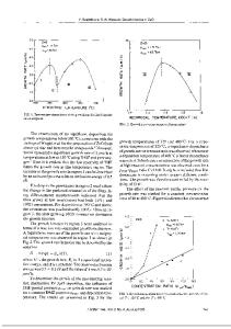
In order to avoid problems with process uniformity that are associated with large Reynolds number (Re) flows, current industrial processes focus on OMCVD in the viscous flow regime at subatmospheric pressure. However, recent developments targeting-group III nitrides, such as Gaxlnl-xN, are limited at present by their high thermal decomposition pressures at their optimum processing temperatures. Because of the high thermal decomposition pressure of InN, OMCVD growth of device quality heterostructures has been limited thus far to Ga-rich alloy compositions. Growth of pure InN at p < 1 atm is restricted to temperatures that represent a poor match to the optimum processing temperature for GaN. Epitaxial growth of InN at higher temperatures has been attempted, but results at p < 1 atm incorporation of indium metal droplets into the InN films [1-3]. Thus fundamental properties of InN are poorly understood for lack of access to high quality crystals or heteroepitaxial layers of this material. Even if the development of GaxInlpxN devices should remain restricted to high gallium concentrations, where thermal decomposition is less of a problem, the lack of knowledge of the fundamental properties of InN must be corrected to support the development of a data base of input parameters for realistic process simulations and to develop an understanding of property - compound stoichiometry relations in the context of device performance and reliability. We have const
Data Loading...