Odmr Measurements of Microcrystalline Silicon
- PDF / 404,040 Bytes
- 6 Pages / 414.72 x 648 pts Page_size
- 3 Downloads / 419 Views
1.0 r
I40 K
Z
hv=2.56 eV
.___0.6 -
0.4-
:3 --
.
x 25
.)ac r° 0.0 0.6
_
front ill. 0.8
1.0
1.2
1.4
1.6
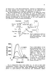
energy (eV) Figure 1: Photo]luminescence spectra of undoped microcrystalline silicon film, recorded with illumination from the front and from the backside. The enlarged trace shows very weak emission at 1.3 eV attributed to a thin amorphous layer at the substrate film interface.
measurements, films of 5 x 10 mm. area and 1-2 prm thickness were placed in an optical transmission resonator and cooled by an Oxford ESR 900 Helium flow cryostat. Optical excitation was done with a Krypton laser tuned at 647 nm and coupled into a optical glass fiber positioned before the entrance funnel of the microwave cavity, so that approximately 30 mW illuminate the sample. This corresponds to an excitation density of approximately 10"1 cm-'. The X-Band microwave was modulated by a p-i-n diode in the CW arm of a Bruker ESP380E spectrometer at frequencies between 280 Hz and 24 kHz. A nitrogen cooled Ge detector (Northcoast E0817) was used for the detection. For the ODMR measurements the total luminescence was used with a cut-off crystalline silicon filter, so that the spectral response E was limited to 1. 10 eV > E > 0.7 eV. The detector signal was fed into a lock-in amplifier; lock-in integration times were chosen at I s and sweep times were 1300 s or 2600 s. Both in-phase (0°) and quadrature signals (90') relative to the microwave modulation were recorded simultaneously, which enables evaluation of the ODMR lifetimes through the r-esponse to a variation of the microwave frequency modulation. RESULTS Photoluminescence (PL) spectra of the films prepared at plasma excitation frequencies from 13 - 95 MHz show an increase of the PL-peak energy from 0.82 eV to 0.9 eV accompanied by an increasing full width a half maximum from 0. 12 eV to 0. 15 eV [7]. Figure I shows photoluminesence spectra of a sample prepared at 49 MHz. The spectra were recorded illuminating from the film- or from the substrate side. The luminescence peaks at approximately 0.88 eV. Contrary to the samples investigated by Depinna et al. [ 1] and Boulitrop et al. [2], the emission originating from amorphous phase in the film is negligible. Only when illuminating through the substrate, a very weak emission at 1.3 eV can be detected, which from structural investigations we attribute to a thin
788
amorphous incubation layer at the substrate-film interface. Therefore all major effects observed by ODMR should be interpreted as originating from the crystalline regions or the disordered grain boundaries between the crystallites. The amorphous "a-Si:H"-like tissue can be neglected for the interpretation.
10K
g=2.0052
Data Loading...