Hole Drift-Mobility Measurements and Multiple-Trapping in Microcrystalline Silicon
- PDF / 116,131 Bytes
- 6 Pages / 612 x 792 pts (letter) Page_size
- 71 Downloads / 387 Views
A8.10.1
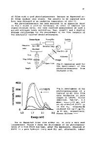
Hole Drift-Mobility Measurements and Multiple-Trapping in Microcrystalline Silicon T. Dylla,1,2 F. Finger,2 and E. A. Schiff1 1 Department of Physics, Syracuse University, Syracuse, NY 13244-1130 USA 2 Institut für Photovoltaik, Forschungszentrum Jülich, Jülich, D-52425 Germany ABSTRACT We present photocarrier time-of-flight measurements of the hole drift-mobility in microcrystalline silicon samples with a high crystalline volume fraction; typical roomtemperature values are about 1 cm2/Vs. Temperature-dependent measurements are consistent with the model of multiple-trapping in an exponential bandtail. While this model has often been applied to amorphous silicon, its success for predominantly crystalline samples is unexpected. The valence bandtail width is 31 meV, which is about 10-20 meV smaller than values reported for a-Si:H, and presumably reflects the greater order in the microcrystalline material. The hole band-mobility is about 1 cm2/Vs – essentially the same magnitude as has been reported for electrons and for holes in amorphous silicon, and suggesting that this magnitude is a basic characteristic of mobility-edges, at least in silicon-based materials. The attempt-frequency υ is about 109 s-1; this value is substantially smaller than the values 1011 - 1012 s-1 typically reported for holes in amorphous silicon, but the physical significance of the parameter remains obscure. INTRODUCTION There have been several reports of drift-mobility measurements [1,2,3,4] in microcrystalline silicon in the last decade or so since it became clear that this material could be prepared with properties that are interesting for solar cells [5]. There is, of course, an enormous range of possible structures in microcrystalline silicon materials. For each sample there is a spectrum of sizes for the component nano & microcrystallites. Even more poorly understood, for each sample there is also a jumble of non-crystalline material that lies between the crystallites. Unsurprisingly, there has also been a very large spread in reported drift mobilities and transport properties. In this paper we shall first summarize our recent hole drift-mobility measurements in a particular form of microcrystalline silicon that has been developed at Forschungszentrum Jülich as a solar cell absorber, and for which cells with 8.7% conversion efficiency have been reported [6]. We shall not offer a detailed defense of the measurements here, nor shall we offer an extended review and comparison with previous work on microcrystalline silicon; these will be presented elsewhere. Instead, we emphasize an unexpected aspect of the present measurements, which is that they exhibit the features of “exponential bandtail multiple-trapping.” Since its first successful application to amorphous semiconductors in the early 1980’s (see Tiedje’s review [7]), exponential-bandtail multiple-trapping (usually abbreviated as simply “multiple-trapping” or “MT”) has become the standard approach to analyzing most transport experiments in hydrogenated amorphous silicon (a-Si:H
Data Loading...