Origin and Behavior of Main Electron Traps in Si-Implanted GaAs
- PDF / 510,680 Bytes
- 6 Pages / 420.48 x 639 pts Page_size
- 89 Downloads / 257 Views
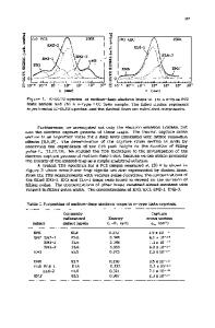
ORIGIN AND BEHAVIOR OF MAIN ELECTRON TRAPS IN Si-IMPLANTED GaAs Z-Q. FANG H. YAMAMOTO AND D.C. LOOK Physics Department, Wright State University, Dayton, OH 45435 ABSTRACT 7 3 The electron traps in Si-implanted active layers(n-101 cm- ) have been studied by capacitance and conductance DLTS techniques in conjunction with different anneal conditions, which include rapid thermal anneals at different temperatures and furnace anneals with a Si 3N4 cap or capless in an AsH3 atmosphere. As compared to the electron traps in as-grown bulk n-GaAs 16 (n-4xI0 cm- 3), nearly the same electron traps, i.e. EL2, EL3, ELM, EL5, EL6 and EL9 can be observed in the Si-implanted layers. Through a comparison with the annealing behavior of the main elect ron traps in bulk n-GaAs, the processing associated origins of some of the traps(EL2, EL3, EL4, EL5 and EL9) observed in Si-implanted GaAs layers have been determined. For some Si-implanted GaAs capped with Si 3N4 and furnace annealed, traps EL3 and EMA dominate the trap EL2. In such layers it is found that emission due to EL3 is reduced while emission from EL12 is 3 augmented by increasing the filling pulse width from 10 gs to 5x10 ts. This phenomenon can be explained in terms of a defect reaction enhanced by electron capture, showing a metastability or bistability.
1. INTRODUCTION The traps in Si-implanted GaAs are of much concern, since they play a significant role in the performance of GaAs IC's and MESFET's, affecting such issues as back/side gating, isolation, variation of threshold voltage, frequency-dependent drain conductance and gate transconductance, and low frequency noise properties [1]. Another concern is the activation efficiency of the Siimplant, which can cause a variation of threshold voltage not only across a wafer, but also along an ingot and from ingot to ingot. The activation efficiency is affected by the crystal stoichiometry and the annealing conditions [2,3]. As a means for qualifying semi-insulating(SI) GaAs boules used for GaAs IC and MESFET fabrication, a standard ion-implantation and anneal cycle has been 12 2 29 proposed. The standard consists of a 2x10 cm- , 150 keV Si implantation followed by an 850'C furnace anneal(FA), using a GaAs proximity wafer, in an inert-gas atmosphere. However the rapid thermal anneal(RTA) process, which is now used by many device manufacturers, has recently been shown to often produce higher activation efficiency than FA [4]. Thus, an understanding of the traps and their possible origins in Si-implanted GaAs activated by RTA is desirable. For the purposes of this paper, we report a comparison of traps in Si-implanted GaAs activated by using different anneal conditions, which include RTA at different temperatures with different proximity wafers(Si vs. GaAs), and FA in an AsH 3 ambient, and traps in bulk n-GaAs before and after FA in a sealed ampoule with a GaAs proximity wafer. It turns out that nearly the same trap species exist in Si-implanted GaAs as in bulk n-GaAs. For some Si-implanted GaAs activated by FA with Si 3 N4 encaps
Data Loading...