Passivation of Zn-Acceptors in InGaAs During Rie with CHF 3 /H 2 and CH 4 /H 2
- PDF / 201,949 Bytes
- 5 Pages / 420.48 x 639 pts Page_size
- 81 Downloads / 348 Views
PASSIVATION OF Zn-ACCEPTORS IN InGaAs DURING RIE WITH CHF 3/H2 AND CH 4/H2
MARTIN MOHRLE Heinrich-Hertz-Institut fUr Nachrichtentechnik Berlin GmbH, Einsteinufer 37, D-1000 Berlin, Federal Republic of Germany
ABSTRACT Reactive ion etching of highly Zn-doped InGaAs with hydrogencontaining gases such as CHF 3/H2 , CH 4/H2 and CH 4 /He leads to a drastical reduction of the concentration of electrically active acceptors in a nearsurface layer. Ti/Pt/Au contacts applied on as-treated p*÷-InGaAs layers show non-ohmic I/V-characteristics due to this passivation effect. Annealing at moderate temperatures (330'C, 20 minutes) was found to restore full electrical activity.
Introduction Passivation of shallow acceptor impurities by atomic hydrogen is known as a general effect in elemental and compound semiconductors. Passivation of acceptors has been observed in Zn-doped GaAs [1] and InP [2]. In both cases samples were treated in a pure hydrogen plasma. De-activation of acceptors in Zn-doped InP resulting from reactive ion etching with CH 4 /H2 has recently been reported [3]. However, no similar effects in InGaAs have been published up to now. In this paper clear acceptor passivation also etching using a variety of passivation effect on the InGaAs will be pointed out.
evidence is presented of the occurrence of in this ternary material during reactive ion hydrogen containing gases. The impact of this formation of non-alloyed ohmic contacts to p-
Experimental InGaAs layers (LPE) either epitaxially doped with Zn to 1.1019 cm- 3 or doped by Zn-diffusion to =1020 cm" 3 were used in this study. The samples were subjected to reactive ion etching in a parallel-plate reactive ion etching (RIE) system operating at 13.56 MHz. Various etching gases such as CHF 3/H2 (95%/5%), CHF 3 , CF4 , CF4/0 2 (95%/5%), CF4/Ar (95%/5%) which are commonly used for the etching of dielectric films such as Si0 2 but which inevitably attack the exposed semiconductor layer underneath when ensuring complete etching, were investigated. In addition, the gas mixtures CH 4/H2 (7%/93%) and CH 4/He (7%/93%) were tested which are employed in the well-established methane RIEprocess for the etching of InP, InGaAs and InGaAsP. In the case of the former gases the experiments were carried out at a fixed gas pressure of 1.2 Pa and a RF power density of 0.16 Wcm" 2. The respective values of the methane-based RIE processes were 10 Pa and 0.41 Wcm- 2 . The cathode involved was water-cooled and good thermal contact to the etched samples was ensured. To measure the electrically active acceptor concentration conventional electrochemical C-V-profiling was used.
Mat. Res. Soc. Symp. Proc. Vol. 163. ©1990 Materials Research Society
496
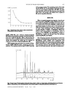
Results on Passivation In fig. I the hole concentration profiles measured on a diffused InGaAs layer before and after a 3 min exposure to a CHF 3/H2 plasma (etching rate < I nm/min) are depicted.
1021
~--20 "0 S101
Fig. 1: Hole concentration in highly doped p-InGaAs before and after RIE with CHF 3/H2 (3 min)
10
1018
0
0.1 02 depth /
Data Loading...