Schottky Barrier Heights of Ni, Pt, Pd, and Au on n-type GaN
- PDF / 240,904 Bytes
- 5 Pages / 414.72 x 648 pts Page_size
- 40 Downloads / 335 Views
3 of sapphire substrates. Hall measurements revealed a bulk carrier concentration of -1017 cmdue to unintentional doping. The room temperature electron mobility was measured to be -250 cm 2 /V-s. A ohmic contact with 300 gm diameter openings was first patterned on the samples.
The ohmic contact consisted of Ti/Al which were deposited by electron beam and thermal evaporation, respectively. The samples were then alloyed in an N2 atmosphere using rapid thermal annealing (RTA). Schottky contacts of 250 gm diameter were patterned at the center of the ohmic contact openings using metal lift-off techniques. The exposed GaN surface was cleaned in the following sequence: descummed in an 02 plasma asher, dipped in diluted HCl, rinsed in DI, and blown-dry with N2. Surface oxides formed in the plasma asher are removed by the HCI solution. The samples were then immediately transferred into an evaporator. Nickel, palladium, and platinum were each deposited by electron beam evaporation, while gold was deposited thermally. The Ni, Pd, and Au were deposited to thicknesses of 100 nm. The Pt, however, was deposited to a thickness of 50 nm due to thermal cracking of thicker layers. The IV characteristics were measured using a four point technique with an HP4142 semiconductor parameter analyzer. An HP4280 was used for C-V measurements at a frequency of 1 MHz. RESULTS AND DISCUSSION The current-voltage measurements were analyzed using the thermionic emission theory. Accordingly, the current-voltage relationship is given by I = Iseq(V-IR)/nkT for V >>kT / q
(1)
and is = AA**T 2 qe-qb/kT
(2)
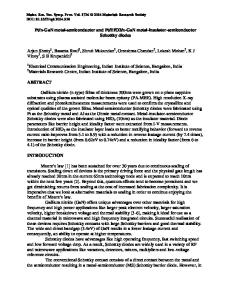
where R is the series resistance, n is the ideality factor, T is the measurement temperature, A is the area of the diode, A** is the effective Richardson constant, and Ob is the effective barrier height. An effective electron mass of mn = 0.22mo was used to determine the theoretical value of the Richardson constant which is 26.4 A cm-2 K- 2 [4]. When R is small, a log I vs. V plot of the forward characteristics yields a linear region in which a fit can be used to calculate the barrier height and ideality factor from the y-intercept and slope, respectively. Figure 1 shows the forward characteristics (Log I vs. V) of the four metals investigated in this work. For Ni, Pt, Pd, and Au, the barrier heights are 0.95, 1.01, 0.94, and 0.87 eV, respectively, while the ideality factors are 1.04, 1.05, 1.04, and 1.04, respectively. The electron affinity, Xs, is determined using the relation Xs = ým - Obb.The metal work function, 0m, is 5.15 eV for Ni, 5.65 eV for Pt, 5.12 eV for Pd, and 5.1 eV for Au [5]. Therefore, the electron affinity from I-V measurements for Ni, Pt, Pd, and Au are 4.20, 4.64, 4.18, and 4.23 eV, respectively.
832
10-3 10-4 10-5 , 10-6 10-7
S108 10.9 10-10 10-11 0.7
0.6
0.5
0.4
0.3
0.2
0.1
Applied Bias (V) FIG. 1. Forward Log I vs. V characteristics for Ni, Pt, Pd, and Au Schottky barrier contacts. The reverse I-V characteristics of the four metals are shown in Figure 2. The reverse bias leakage current for the Ni and Pd diode
Data Loading...