Pitting Sites on Al Controlled by Microcontact Printing Using Poly(chloroprene) Rubber Mask Film
- PDF / 190,538 Bytes
- 1 Pages / 612 x 792 pts (letter) Page_size
- 85 Downloads / 306 Views
of the microcapsules from ~4.5 μm to ~3 μm and significantly increases the structural integrity of the capsules, which is attributed to the increase in wall thickness that accompanies the shrinking. They verified the structural integrity of the thermallytreated microcapsules by noting the percentage of capsules that were not deformed upon ingestion by cells; the capsules with thicker walls are reinforced and thus are more suited to the delivery of encapsulated materials. Using optical transmission microscopy, the researchers demonstrated the activation of a microcapsule inside a cancer cell using a laser with a wavelength of 830 nm and an incident intensity of 50 mW. The capsules had silver nanoparticles (diameter > 20 nm) embedded in the walls, but had no encapsulated material. Silver nanoparticles were chosen in part because they absorb the 830 nm light and in part because they provide dark contrast in the optical transmission microscope. The researchers also performed release experiments on AF-488 dextran encapsulated microcapsules that had gold or gold sulfide nanoparticles embedded in the walls. These studies showed that ingested living cells adhere to the substrate both before and after the release of the encapsulated polymer, demonstrating that this method is feasible for the delivery of materials into specific cells. The studies also showed that microcapsules that were merely adhered to the outer membrane were lifted up and away from the cells during illumination and were not disrupted, demonstrating that only the ingested microcapsules release their encapsulated material upon irradiation. THAD AWEEKA
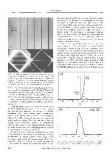
siloxane) (PDMS) on a metal mold with an ideally ordered array of convex protrusions on its surface and cured it for 12 h at room temperature. After they mechanically detached the PDMS hole array (stamp) from the metal mold, the researchers dipped the stamp in a 1 wt% toluene solution of CR and pulled it at a constant rate. When the toluene evaporated, a thin CR film was formed on the stamp. They then transferred the CR film on the stamp to an Al foil through physical contact and detachment since the adhesion of CR to Al is much stronger than to PDMS. They then etched the Al foil covered with the patterned CR film in HCl solution under a constant dc current condition. The CR film printed on the Al foil masks against the anodic etching of the Al so that no pits are initiated on the CR film. Using this method, the researchers fabricated uniform pits arranged in an ideal array over the Al film with the same 〈100〉 orientation, a width of ~3 μm, a depth of ~1.5 μm, and an interval of 5.0 μm. While the width and interval of the pits can be precisely controlled, the researchers could not control the depth of the pits, because prolonged etching induces a substantial dissolution of the sidewalls of the pits. Further study is needed to make the pits sufficiently deep. The researchers said that using this process, they can optimize the surface area of an Al electrode for electrolytic capacitors by forming ordered arrays
Data Loading...


