Planarization of Copper Damascene Interconnects by Spin-Etch Process: A Chemical Approach
- PDF / 386,112 Bytes
- 6 Pages / 612 x 792 pts (letter) Page_size
- 71 Downloads / 374 Views
Planarization of Copper Damascene Interconnects by Spin-Etch Process: A Chemical Approach Shyama P. Mukherjee, Joseph A. Levert Honeywell Electronic Materials, 1349 Moffett Park Dr., Sunnyvale, CA, USA Donald S. DeBear, SEZ America Inc, 4824 South 40th St., Phoenix, AZ 85040, USA ABSTRACT The present work describes the process principles of “Spin-Etch Planarization” (SEP), an emerging method of planarization of dual damascene copper interconnects. The process involves a uniform removal of copper and the planarization of surface topography of copper interconnects by dispensing abrasive free etchants to a rotating wafer. The primary process parameters comprise of (a) Physics and chemistry of etchants, and (b) Nature of fluid flow on a spinning wafer. It is evident, that unlike conventional chemical-mechanical planarization, which has a large number of variables due to the presence of pads, normal load, and abrasives, SEP has a smaller number of process parameters and most of them are primary in nature. Based on our preliminary works, we have presented the basic technical parameters that contribute to the process and satisfy the basic requirements of planarization such as (a) Uniformity of removal (b) Removal rate (c) Degree of Planarization (d) Selectivity. The anticipated advantages and some inherent limitations are discussed in the context of process principles. We believe that when fully developed, SEP will be a simple, predictable and controllable process.
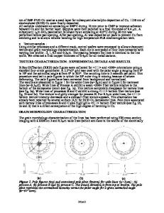
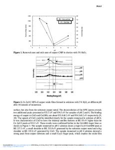
INTRODUCTION Copper dual damascene architectures are increasingly being used for interconnects in integrated circuits. The copper is electrodeposited with processes that generate a nonplanar surface [1]. The current method for the planarization of copper dual damascene features and their underlying barrier metals is Chemical-Mechanical Planarization (CMP) process [2]. In CMP processes, the mechanical forces play a dominant role. The present work describes an emerging method of planarization called “Spin-Etch Planarization” (SEP). This is a chemical approach involving no mechanical force. The process involves the uniform removal as well as planarization of copper surface topography by dispensing abrasive free etchants onto a rotating wafer using a commercial spin-etch tool (SEZ 203) [3,4]. In this context, it is worth referring another chemical approach of planarization called Electrochemical Planarization based on the principle of anodic leveling or electropolishing [5]. This process also does not have applied mechanical forces. We believe that the advent of copper damascene interconnects and the polymeric and nanoporous low-k dielectric are the driving force for chemical approaches. The removal process, of metal as used in SEP, can be described as “controlled” wet chemical dissolution of a metal surface in electrolytes on a rotating wafer. The term “etch “ here should be expressed as a controlled wet “chemical polishing” rather than “etching” which does not fulfill the requirement of smooth surface finish. The wet chemical etching of metals in electrolytes is
Data Loading...