Mechanical Stress Sensors for Copper Damascene Interconnects
- PDF / 620,687 Bytes
- 7 Pages / 612 x 792 pts (letter) Page_size
- 86 Downloads / 453 Views
1052-DD03-01
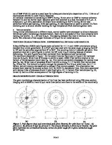
Mechanical Stress Sensors for Copper Damascene Interconnects Romain Delamare1, Sylvain Blayac1, Moustafa Kasbari1, Karim Inal1, and Christian Rivero2 1 Centre de Microelectronique de Provence, GARDANNE, 13541, France 2 STMicroelectronics, ROUSSET, 13106, France ABSTRACT We propose embedded microsensors to investigate the mechanical stress in copper damascene lines in a standard CMOS microelectronic technology. Those sensors are based on the silicon piezoresistive effect where strain in the active silicon is induced by orientated copper lines. The challenge is to correlate the electrical sensors signal directly to stress variation in lines. We have performed electrical measurements of the structures as a function of temperature. A coupled analytical and finite element thermomechanical model of the structure was developed and a good agreement with measurements was obtained. INTRODUCTION It is well known that mechanical stress is developed during manufacturing process of CMOS microelectronic circuits [1]. This residual stress plays an important role in the devices reliability and often generates fabrication yield loss [2]. This phenomenon becomes of increasing importance as the complexity (integration density, number of metal levels, thermal cycling, packaging effects…) grows. It is therefore of major importance to correlate parameters with mechanical stress under systematic control along process to minimize yield losses. Thus, in response to industrial requests, we developed an embedded microsensor for monitoring the local stresses in Copper Damascene interconnects. In the present work, we report results obtained with a new test structure and demonstrates the link between electrical response of the sensor and stress variation in the first metal level. The aim of this paper is to report the results obtained with this embedded structure and demonstrate its relevance as a copper stress sensor. The second part introduces the principles of this piezoresistive sensor. The third part details the electro-thermal finite-element model and shows the comparison with actual measurements. SENSOR DESIGN Sensor fabrication The basic sensitive element is a silicon resistor underneath copper lines. Those lines induce an additional stress on the sensor through the piezoresistive effect (see Figure 1).
Figure 1: SEM cross sectional view of a stressed resistor with seven Copper lines (metal-1 level) and corresponding FEM simulation. The cross section of the structure is made in the (110) plane perpendicular to the resistor main axis. Resistors (p+ doped silicon, [110] oriented, L = 27 µm and W = 2.7 µm) are surrounded by the SiO2 shallow trench isolation (STI). In the silicon dioxide, above the resistor, seven copper lines are grown with a damascene process. The mean distance between silicon and copper lines is 550 nm. These lines are oriented along the long axis of the resistor (27 µm long) and their size is 0.2 µm large, 0.3 µm height (their aspect ratio L / W is 135). The first intermetal dielectric oxide was etched, a
Data Loading...