Power Feeding in Large Area PECVD of Amorphous Silicon
- PDF / 299,633 Bytes
- 6 Pages / 414.72 x 648 pts Page_size
- 99 Downloads / 379 Views
ABSTRACT Plasma processes are usually worked out in a small-scale environment (electrode area maximum 121 cm 2, rf- and VHF- excitation frequencies ). In order to meet the requirements of large area device applications they have to be upscaled. The investigations of glow discharge systems for different PECVD reactors (parallel plate- and coaxial electrodes) have shown, that the reactor design (power supply, line connection) sharply influences the large area deposition process. The voltage distribution on the driven electrode especially determines the uniformity of the deposited layer thickness. Possibilities which influence the voltage distribution on large areas will be discussed. The results of large area electrode description as an electrical line will be discussed in comparison with different reactor configurations and the optimization of the behavior of the deposition process. The experimental results of a coaxial reactor (electrode area 5000 cm 2, substrate length 120 cm) show that a homogenous deposition of amorphous silicon (layer uniformity of thickness over the length better ± 7 %) by connecting the driven electrode with additional electrical devices is possible. EXPERIMENTAL Two different glow discharge systems used for the experiments: PECVD parallel plate glow discharge system ([1]): The parallel plate glow discharge system bases on the plasma box principle. The plasma box consists of a grounded frame and two substrate panels pressed against it from either side to form the box covers. The double-sided rf electrode assembly is arranged centrally between the two substrates with the feed gases admitted through its perforated electrode panels. . The spacing for the plasma produced is 3 cm. The area of the electrode exposed to the plasma is 4200 cm2 . PECVD coaxial glow discharge system: The diameter of the inner electrode of the coaxial glow discharge system is 12 cm and the area of the electrode exposed to the plasma is 4500 cm 2. The spacing for the plasma produced is 4 cm. The gas flows through a porous grounded electrode into the plasma chamber. Pressure ranging from 10 to 40 Pa was used for nitrogen and silane discharges. To minimise the dust in the plasma during high rate deposition of a- Si:H from silane a maximal gas flow rate up to 2400 Pal/s was used. The coaxial capactive coupled radio-frequency discharge at 13.56 MIL1z allows a-Si:Hdeposition rates up to 20 jtm/hr ([2]).
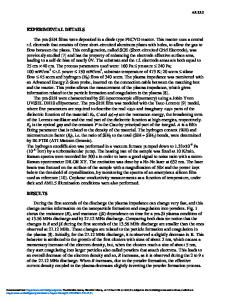
PROBLEMS Using Very High Frequencies (VHF) or processing with large area substrates the dimensions of the electrodes obtain quickly the dimensions of the wavelength X. In this case the reactor 27 Mat. Res. Soc. Symp. Proc. Vol. 377 ©1995 Materials Research Society
shows the behavior of as a transmission line. Because of the open circuited end of the line a standing wave is generated on the surface of the electrodes and on the feed lines (Fig. 1).
Fig. 1: A standig wave on the electrode and the feed line (the length of the electrode is X/4)
Fig. 2: Standig wave on a electrode with capacitive loading
The potential in Figure
Data Loading...