Process Optimization for Multiple-Pulses Laser Annealing for Boron Implanted Silicon with Germanium Pre-amorphization
- PDF / 157,322 Bytes
- 6 Pages / 612 x 792 pts (letter) Page_size
- 3 Downloads / 374 Views
D6.19.1
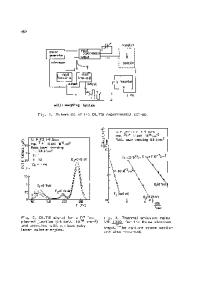
Process Optimization for Multiple-Pulses Laser Annealing for Boron Implanted Silicon with Germanium Pre-amorphization Debora Poon, Byung Jin Cho, Yong Feng Lu, Leng Seow Tan, Mousumi Bhat1 and Alex See1 Silicon Nano Device Laboratory and Laser Micro-processing Laboratory, Department of Electrical and Computer Engineering, National University of Singapore, 10 Kent Ridge Crescent, Singapore 119260. 1 Technology Development Department, Chartered Semiconductor Manufacturing, 60 Woodlands Industrial Park D, Street 2, Singapore 738406. ABSTRACT One of the major advantages of multiple-pulses Laser Thermal Annealing (LTA) with moderate energy fluence is that good dopant activation can be achieved without further increases in junction depth by successive pulses. It is demonstrated that when the laser fluence is adjusted to a value that can melt the preamorphization implantation (PAI) layer but not the underlying silicon substrate, PAI layer depths control the junction depths. Hence, it is desirable to operate LTA in this regime since this allows for a tighter process control as opposed to when the junction depth is controlled solely by the laser fluence. High Resolution Transmission Electron Microscopy (HR-TEM) micrographs show that the degree of damage repair depends on the amorphous layer thickness as well as the number of pulses. Our study allows for the evaluation of the maximum allowable PAI depth for a given number of pulses in order to fully remove the damage caused by the PAI. INTRODUCTION As the gate length of MOSFET decreases, an ultrashallow and abrupt junction is required to suppress short-channel effects and reduce parasitic resistances. A PAI followed by sub-keV boron implantation is one of the most promising candidates to form p+/n ultrashallow junctions owing to its ability to suppress the channeling tail of boron [1]. Amorphization can be accomplished by implanting ions of silicon, the noble gases, germanium, tin and indium [2]. The major problem of the preamorphization method however, is that the presence of residual defects formed below the original amorphous/ crystal interface would drastically increase the leakage current when the defects are contained within a depletion layer of the operating device [3]. For 65 nm technology and below, LTA combined with low energy boron implants and preamorphization is one of the likely solutions to junction requirements [4]. It has previously been shown that amorphization of the wafer surface prior to laser anneal can provide a process window in laser fluence over which the junction depth is limited by the amorphous depth [5]. Poon et. al. reported that multiple-pulses laser annealing of preamorphized silicon with moderate energy fluence can achieve a defect-free junction with a good degree of activation of boron without compromising the junction depth [6]. In this paper, we attempt to come up with a model that allows for the prediction, from four-point probe measurements, of the maximum allowable PAI depth for a given number of pulses in order to fully remove
Data Loading...