A Nucleation Study of GaN Multifunctional Nanostructures
- PDF / 137,677 Bytes
- 6 Pages / 612 x 792 pts (letter) Page_size
- 12 Downloads / 313 Views
E12.7.1
A Nucleation Study of GaN Multifunctional Nanostructures Gupta, Shalini1, Kang, Hun1, Strassburg, Martin1,2, Asghar, Ali1, Senawiratne, Jayantha 2, Dietz, Nikolaus 2, Ferguson, Ian T.1,3,∗ 1
Georgia Institute of Technology, Electrical and Computer Engineering, Atlanta, GA 30332, U.S.A.
2
Georgia State University, Department of Physics and Astronomy, Atlanta, GA 30303, U.S.A.
3
Georgia Institute of Technology, School of Materials Science and Engineering, Atlanta, GA 30332, U.S.A.
ABSTRACT This paper reports the Metal Organic Chemical Vapor Deposition (MOCVD) growth of GaN nanostructures. The use of MOCVD allows the direct integration of these nanostructures into pre-existing device technology. The formation of GaN nanostructures grown on AlN epitaxial layers were studied as a function of growth temperature, growth rate, V-III ratio and the amount of deposited material. A wide range of temperatures from 800 °C to 1100 °C and V-III ratios from 30 to 3500 were applied to determine the optimal growth conditions for nucleation studies in a modified production reactor. Small GaN nanostructures with lateral dimensions below 50 nm and low aspect ratios were obtained using relatively low temperatures of 815 °C and extreme metal-rich growth conditions. Island densities up to 1010 cm-2 were achieved using silane as an anti-surfactant to increase the available nucleation sites. Manganese has been incorporated into these nanostructures to enhance the multifunctional ferromagnetic properties of GaMnN. INTRODUCTION Opto-electronic devices based on the wide band-gap material GaN and its ternary compounds with indium and aluminum have been found to show promise in commercial applications such as ultra violet lasers, white light emitting diodes, ultra sensitive detectors, and field effect transistors for high power operations [1]. In addition, III-Nitrides have recently drawn attention because of their potential for spintronics applications since the incorporation of transition metal (TM) ions can provide room temperature ferromagnetism [2]. Nanostructures have been shown to enhance the performance and efficiency of optoelectronic devices. The control of the lattice site where the TM ions are incorporated is also desirable to optimize ferromagnetism. Thus, the potential of the GaN/AlN hetero-system for the fabrication of multifunctional nanostructures that have both enhanced optical and electrical properties need to be explored. Self-organized growth modes of ∗
Corresponding author: [email protected]
E12.7.2
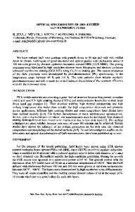
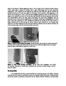
quantum dots are proven to provide arrays of nanostructures similar in size and shape with densities ranging between 108 to 1012 cm-2 [3, 4]. The lattice mismatch between GaN and AlN is ~2.5 %, thus the formation of nanostructures in a Stranski-Krastanow (SK) like growth mode is not supported. For GaN/AlN heterostructures a 3D growth by a ripening process producing islands with infinite size is predicted according to the evaluation of the free surface energy [5]. However, GaN nanostructures were recently demon
Data Loading...