Characterization of Light Emission from 4H and 6H SiC MOSFETs
- PDF / 239,062 Bytes
- 6 Pages / 612 x 792 pts (letter) Page_size
- 53 Downloads / 338 Views
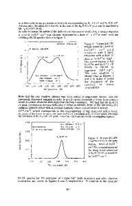
Characterization of Light Emission from 4H and 6H SiC MOSFETs P.J. Macfarlane and R.E. Stahlbush Naval Research Laboratory, Code 6816, 4555 Overlook Ave SW, Washington, DC 20375 U.S.A ABSTRACT While SiC devices are an attractive alternative to Si in high power applications, interface trap densities measured in SiC-based MOSFETs are significantly larger than in Si-based ones. Here, we study SiC MOSFETs using both spatial images and spectral analysis of light emission due to electron-hole recombination. The light emission is produced by alternately driving the channel between accumulation and inversion using what is essentially a charge-pumping set-up. Emission is due to interface trap and bulk electron-hole recombination. The spatial imaging studies suggest that recombination occurs at both interface traps and bulk defects. Spectral studies of the emission indicate the presence of a narrow band centered at 425 nm and a broad band extending from approximately 500 to 800nm. The former we suggest is due to bulk recombination and the latter to interface trap recombination. The spectral studies of the 500 to 800 nm band are timed to separate light emitted during the inversion-to-accumulation transition from that emitted during the accumulation-to-inversion transition and visa versa. Comparisons of the emission spectra collected during these specific periods are consistent with a larger Dit in the upper half of the bandgap than the lower half in both 4H and 6H devices. INTRODUCTION SiC has a wide bandgap, high breakdown field, and high thermal conductivity making it an attractive replacement for Si in high power, high temperature applications. SiC is the only wide bandgap semiconductor whose native oxide is SiO2. Thus, there is the potential to create a SiC metal-oxide-semiconductor field-effect transistor (MOSFET) using processing methods similar to those used to create the Si-based MOSFET. However, the development of a SiC-based MOSFET has been hampered by the lower than predicted minority carrier channel mobility observed in the current technology. The low mobility is thought to be due to the high interface trap densities observed in these materials, which is particularly large in 4H SiC MOSFETs.1 Here we image light emission due to electron-hole recombination at both interface traps and bulk defects. Other descriptions of this method can be founds in refs. 2 and 3. In addition to the spatial information from the emission images, we present spectral studies of the light emission. By using a temporal separation of emission processes, it is possible to separate emission of interface traps in the top half of the bandgap from emission due to interface traps in the bottom half. While an exact correlation cannot be made between the intensity of the emission spectra and energy distribution of interface traps, some general observations about the light emission from interface traps can be garnered. It is observed that while in both 4H and 6H MOSFETs more interface traps have states in the upper half of the bandgap, and in the 4H
Data Loading...