Characterizations of Boron Carbon Nitride and Boron Carbide Films Synthesized by PECVD
- PDF / 181,184 Bytes
- 6 Pages / 612 x 792 pts (letter) Page_size
- 87 Downloads / 407 Views
1108-A09-28
Characterizations of Boron Carbon Nitride and Boron Carbide Films Synthesized by PECVD Qingguo Wu, Mandyam Sriram, Jim Sims, Haiying Fu, Sesha Varadarajan and Tim Archer PECVD Business Unit, Novellus Systems, Inc., 11155 SW Leveton Dr. Tualatin, OR 97062
Nathan J. Trujillo and Karen K. Gleason
Department of Chemical Engineering, Massachusetts Institute of Technology, Cambridge, MA 02139
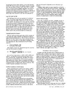
ABSTRACT Thin films of boron carbon nitride (BCN) and boron carbide (BC) were synthesized by plasma enhanced chemical vapor deposition (PECVD) using two different reactant chemistries: (i) N,N’,N” – trimethylborazine (TMB); (ii) dilute diborane (5% in Ar) and hydrocarbon as precursor materials. Fourier transform infrared spectroscopy (FTIR), Raman spectroscopy, Nano-Indentor, Flexus stress instrument and x-ray photoelectron spectroscopy were used to study the deposited films. The BC films are much more stable than BCN films under high humidity (100%) environment. Both BCN and BC films are very stable under atmospheric conditions. A high compressive stress of -4.2 GPA was achieved by conventional PECVD, which show promising applications in high performance ultra large-scale integrated circuit (ULSI) devices. INTRODUCTION Recently there has been great interest in depositing boron carbon nitride (BCN) and boron carbide (BC) films because they exhibit many attractive properties for thin film applications. They are expected to have excellent mechanical properties similar to diamond, cubic boron-nitride (c-BN), and carbon-nitride (β-C3N4) [1], and they have low dielectric constant and high compressive stress under certain conditions.[2-6] In general, low dielectric constant is achieved through co-deposition of a backbone precursor and a porogen. The porogen is driven out during a cure step, leaving the backbone and increased free space behind.[7] This free space can lead to degraded mechanical properties of the film relative to fully dense materials. It also allows for penetration of moisture and solvents during integration, potentially worsening the interconnect performance.[8,9] Sugino et al and Liu et al, respectively, reported a polycrystalline boron carbon nitride (BCN) film with dielectric constant as low as 2.1-2.4 without using porogen.[2-4]. In addition, Lousa et al presented high stressed boron carbide thin films deposited by tuned-substrate RF magnetron sputtering and using pure solid B4C as precursor. However, repeatable film thickness and uniformity may be difficult to obtain with this method due to the use of a solid precursor and the fact that the active solid surface area changes during deposition. Stressed silicon nitride films have been used as spacers or middle-of-the-line (MOL) liners, also known as pre-metal dielectric (PMD) liners. To improve drive current in complementary metal oxide semiconductor (CMOS) devices, highly stressed films are needed. Many efforts have been made in recent years to develop high compressive and high tensile
stressed films, including the investigation of precursors and depo
Data Loading...