Contact Issues of GaN Technology
- PDF / 999,501 Bytes
- 8 Pages / 417.6 x 639 pts Page_size
- 90 Downloads / 344 Views
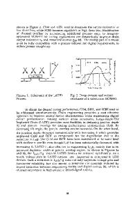
to the presence of the piezoelectric donor charge at the AIGaN/GaN interface 21. Internal photo emission is an alternative way to determine the Schottky barrier height of a metal/AlGaN/GaN heterostructure. In our laboratory, we have measured the barrier height of Ni of A10.15Ga 0 .85N (300 A and 500 A)/GaN using the internal photo emission technique and obtained a barrier height of -1.30 eV, independent of the AlGaN layer thickness131. This value, well within the experimental scattering range, is considered to be consistent with the value obtained on bulk A10. 15Gao.85N samples. As the mole fraction of Al in the AlGaN top layer changes to 30%, the barrier height is seen to increase further to - 1.56 eV (see Table 1). These results suggest that the Schottky barrier of HFET structures is largely determined by the upper most AIGaN layer and that the barrier height appears to increase between 0.25 to 0.3 eV for every 15% increment in Al mole fraction in the AIGaN layer up to 30 % of Al. More work is needed to correlate the barrier height and the Al mole fraction in detail. Table 1. Summary of Schottky barrier height(a) Ideality
q4b (I-V)
q• (I-V)
q4 (C-V)
Metal
Material
n factor
(eV)e)
(eV)f)
(eV)
q4 (photo) (eV)
Ni
Bulk AlGaN(b)
1.23
1.03
1.25
1.26
1.28
Ni
GaN
1.14
0.84
0.95
0.96
0.91
Ni
HFET(c)
1.31
Ni
HFET(d)
1.56
Ti
Bulk AlGaNNb)
1.08
0.79
0.84
1.10
Ti GaN 1.08 0.60 0.65 0.68 (a)The data (I-V and C-V) are the average value from 15 diodes; the standard deviation is about 0.05 for both of the n factor and the barrier heights. (b)A1 mole fraction was 15% in the AIGaN samples. (c)A10. 15Gao.85 N (300 A or 500 A)/3[am undoped GaN. (d) Alo. 3Gao. 7N
(500 A)/3[tm undoped GaN.
(e)Calculated from Equation 1;
I= AA*T 2e-q~b / kU(eqVl/kT
_ Il)
(1)
(f)Calculated from Equation I and corrected by equation 2;
0•b= nob
- (n - 1) UTlnN q Nd
(2)
We have also been investigating the ohmic behavior on the III-V nitrides. Of particular interest to us was understanding how to fabricate low resistance and reproducible ohmic contacts on HFET structures. During the course of the study, we found that the ohmic behavior varied significantly from one wafer to another, even though these wafers were nominally the same, i.e., n- Al0 .15Ga 0.85N (300 A)/ Al0 .15Ga 0 .85N (30 A, undoped)/i-GaN(1 jIm). Table 2 shows the results of the measured contact resistivity on four different wafers with nominally the same structure. The nsp product, extracted from Hall effect measurements, is the usual parameter that characterizes the HFET samples (see Table 2). For samples with a large value of nsji product, the contact resistance should be low, compared to samples with a small nsji value, at least in principle. This is because the nsj product is believed to indicate good electrical conduction in the channel region and should lead to low ohmic contact resistance. According to this idea, sample #4, in Table 2 should yield the lowest contact resistance, since it had the largest value of nsl; and sample 2 with the
Data Loading...