Copper oxide nanoparticles for thin film photovoltaics
- PDF / 319,382 Bytes
- 6 Pages / 432 x 648 pts Page_size
- 8 Downloads / 545 Views
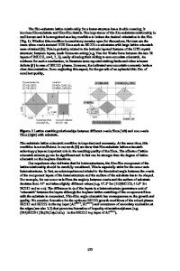
Copper oxide nanoparticles for thin film photovoltaics Maurice Nuys1, Jan Flohre1, Christine Leidinger1, Florian Köhler1 and Reinhard Carius1 1 Institute of Energy and Climate Research 5 -Photovoltaics-, Forschungszentrum Jülich GmbH, D-52425 Jülich Germany ABSTRACT Commercially available tenorite (CuO) nanoparticles (NPs) were investigated in particular with respect to their suitability for photovoltaic applications. NPs with a diameter of about 30 nm were step wise annealed up to 1000°C in nitrogen atmosphere. The influence of the annealing treatment on the structural and electronic properties was investigated by Raman, photoluminescence (PL) and photothermal deflection spectroscopy (PDS) as well as X-ray diffraction measurements. Size, shape, and phase of the untreated NPs are analyzed by TEM measurements. The PL and PDS results show a strong increase of the tenorite band edge emission at about 1.3 eV accompanied by a decreasing sub gap absorption with increasing annealing temperature up to 700°C. According to literature, a phase transition from tenorite to cuprite (Cu2O) was expected and observed after annealing at 800°C. Strong cuprite band edge emission at about 2 eV accompanied by very weak defect and possibly tenorite band edge emission was found for samples annealed at 800°C and 1000°C. INTRODUCTION The long term objective for the world wide installation of photovoltaic systems is far beyond 10TW. A sustainable development asks for photovoltaics based on almost unlimitedly available elements. Up to now, silicon based materials already fulfill this requirement but further improvements in efficiency and cost reduction can only be achieved by multi-band gap thin film solar cells. We have investigated copper oxide based nanoparticles (NPs) for their feasibility as a new absorber material in thin film solar cells. Tenorite and cuprite show optical band edges at about 1.35 eV to 1.5 eV and 2.1 eV, respectively, which is in the range for a reasonable photovoltaic application [1-4]. Especially cuprite had been intensively investigated regarding its potential as an absorber material in solar cells due to its suitable optical band gap, cheapness, and abundance [5, 6]. However, poor material properties due to high defect concentration and the formation of metallic copper at the surface were crucial parameters leading to a fading interest in cuprite for photovoltaic application. Recently, copper oxide regained attention as absorber material in thin film solar cells [7]. Using NPs instead of thin films is a promising approach to overcome problems of the past. For instance, phase pure and almost defect free NPs are prepared more easily compared to thin films. Moreover, NPs may favor a self-purification process, where the impurities and material defects tend to diffuse to the surface upon thermal annealing. In the present study, tenorite NPs were step wise annealed in nitrogen atmosphere. The impact of this treatment on the electro-optical and structural properties was investigated by Raman and photoluminescence (PL) spec
Data Loading...