Crystalline and Electrical Properties of ITO Semiconductive Films deposited by Atmospheric RF Plasma Technique
- PDF / 853,417 Bytes
- 5 Pages / 414.72 x 648 pts Page_size
- 31 Downloads / 379 Views
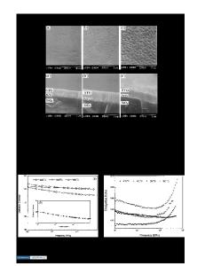
of one. A standard antimony solution (Sb = 0.08213 Molar) was used as the Sb source, with Sb/(In+Sn) ratio of approximately 8%. After stirring, a precursor solution was poured into a plastic container housed in an ultrasonic nebulizer. Excited by the ultrasonic energy, mist was produced from the solution, fed into the plasma reactor, where it was then completely evaporated. The resultant vapor was deposited onto the substrate outside of the reactor. The precursor material feeding rate, or mist rate, was varied between 0.10 to 0.13 ml/min. Oxygen gas flow was introduced through either the tangential plasma gas inlet or the carrier gas inlet. Most films reported in the following section were fabricated with the tangential oxygen flow rate of 5 1/min., and the oxygen carrier gas flow rate of 4 I/min. The substrate temperature was 500 'C, and the deposition time was 60 min. Substrate materials were soda-lime-silicate (SLS) float glass and fused silica glass. The as-deposited films coated on the substrates were adhesive, and subsequently analyzed. RESULTS The films were nearly 100% transparent in the visible region. Elemental analysis showed that the initial stoichiometric ratios of In:Sn in the precursor solution are close to that of the films.
851 Mat. Res. Soc. Symp. Proc. Vol. 452 0 1997 Materials Research Society
r
'Mist
Carrier Gas
,',
Inlet (Ar)
I•Solution
9I 41
I
S
aIlt
Plsm
EI0
10
Flame
-
UltrasonicNebulizer
arting Material Assembly •lasma Reactor Assembly
a
S~HeaterBlock "- Substrate Assembly Substrate Holder
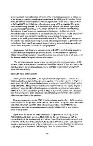
Figure 1. Experimental setup for atmospheric RF plasma mist deposition technique. To study the crystal formation and lattice parameter, X-ray diffraction (XRD) was utilized to analyze films deposited on SLS glass. When the In:Sn ratio was between 10:0 and 6:4, cubic indium oxide (In 2 0 3, ICDD No. 6-4 16, a = 10.118 A) was formed. When the In:Sn ratio was between 4:6 and 0:10, tetragonal tin oxide (SnO2, ICDD No. 21-1250, a = 4.738 A, c = 3.188 A) was formed. Thus, the phase transition from the In20 3 to the SnO2 phase took place between In:Sn = 6:4 and 4:6 in the film samples. As tin was doped into cubic In 20 3, the location of a characteristic diffraction peak shifted to lower angles, indicating a lattice parameter expansion. The lattice parameter, a, increased as the tin concentration increased, see Figure 2. The total relative shift was approximately 0.78%/'. On the other hand, when indium was doped into tetragonal Sn0 2 , lattice parameters, a and c, changed slightly, see Figure 3 (a) and (b) respectively. Such trends in those cubic In 20 3 and tetragonal SnO2 films are consistent with that of previously determined powder samples[3]. 10.220 10.200 ci) 10.180
a) E 10. 160 Co 10. 140 0.
ci) 10.120 C, Co
10.100 -10
0
10
20
30
40
50
tin concentration (mol %)
Figure 2. Lattice parameter, a, for cubic indium oxide films 852
with increasing tin concentration.
(a)
CUU) U)
4.755 4.750 4.745
E 4.740 4.735
Cu CU 0 U) C.) CU
4.730 4.725 50
60
70
80
90
100
110
10C
Data Loading...