Properties of Nano-crystalline n-type Silicon Films Produced by Hot Wire Plasma Assisted Technique
- PDF / 6,238,958 Bytes
- 6 Pages / 612 x 792 pts (letter) Page_size
- 44 Downloads / 354 Views
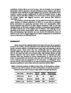
Properties of Nano-crystalline n-type Silicon Films Produced by Hot Wire Plasma Assisted Technique I. Ferreira, F. Braz Fernandes, P. Vilarinho1, E. Fortunato and R. Martins, Departamento de Ciência dos Materiais, CENIMAT, Faculdade de Ciências e Tecnologia da Universidade Nova de Lisboa and CEMOP/UNINOVA, Quinta da Torre 2828-114 Caparica, Portugal. 1 Departamento de Cerâmica e do Vidro, UIMC, Universidade de Aveiro, 3810-193 Aveiro, Portugal. ABSTRACT In this work, we present the properties of n-type silicon films obtained by hot wire plasma assisted technique produced at different rf power and gas flow rate. The films were produced at a filament temperature of 2000ºC and the rf power was varied from 0W to 200W while gas flow rate was varied from 15 to 100sccm keeping rf power at 50W. In this flow rate range, the growth rate of the films varied from 5Å/s to 250Å/s and the corresponding electrical room dark conductivity varied from 10-2 to 10(Ωcm)-1. On the other hand, we observed that the electrical conductivity increased from 2 to 6(Ωcm)-1, and the Hall mobility from 0.1 to 2cm2/V.s as rf power change from 0W to 200W. The infrared, EDS and XPS analyses revealed the existence of oxygen incorporation, which is not related to post-deposition oxidation. The X-ray diffraction and µRaman data show the presence of Si crystals in the films structure and the SEM micrographs reveal a granular surface morphology with grain sizes lower than 60nm. INTRODUCTION Plasma assisting hot wire process to produce amorphous and nanocrystalline silicon films was introduced with success by the authors in 1998 [1]. The deposition system was designed in such way that permits the production, in the same reactor, of films by plasma enhanced chemical vapor deposition (PE-CVD), hot-wire chemical vapor deposition (HW-CVD) or both techniques simultaneously, that we designated by hot-wire plasma assisted chemical vapor deposition (HWPA-CVD). The HWPA-CVD technique takes the advantage of PE-CVD to produce compact films and the advantage of HW-CVD to enhance the films growth rate. Therefore, using HWPACVD technique it is possible to produce compact films at high growth rate [2]. This study deals with the influence of rf power (P) and gas mixture flow rate (f) on the electro-optical, and structural properties of n-type nano-crystalline silicon films. The onset deposition conditions for this study were those obtained for the production of optimized n-type films by HW-CVD technique [3]. From that, we add an rf power to the process and we studied its influence on the properties of the obtained films. EXPERIMENTAL Details concerning the deposition system used to produce the n-type films analysed in this work are described elsewhere [3]. The gas mixture used for the process is from a pre-mixed gas bottle containing 0.7%PH3, 15.1%SiH4, and 2%H2 diluted in He. During the deposition, the filament temperature (Tf) was set to 2000ºC, the gas pressure (p) to 0.8 Torr for a hydrogen A7.6.1
dilution of 87%, and the substrate temperature (Ts) to 200ºC. P was va
Data Loading...