Curvature and strain in thick HVPE-GaN for quasi-substrate applications
- PDF / 444,847 Bytes
- 5 Pages / 612 x 792 pts (letter) Page_size
- 82 Downloads / 252 Views
Y2.11.1
Curvature and strain in thick HVPE-GaN for quasi-substrate applications Claudia Roder1, Tim Böttcher1, Tanya Paskova2, Bo Monemar2, Detlef Hommel1 University of Bremen, Institute of Solid State Physics Otto-Hahn Allee, 28359 Bremen, Germany 2 Linkoeping University, Department of Physics and Measurement Technology 581 83 Linkoeping, Sweden 1
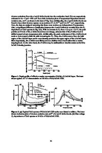
ABSTRACT Uncracked HVPE-GaN layers of different thicknesses were investigated using high resolution x-ray diffraction at variable temperatures. The absolute lattice parameters as well as the wafer curvature were measured simultaneously at different temperatures. All samples were found to be under biaxial tension at growth temperature. At room temperature the GaN film is under biaxial compression while the substrate is tensile strained. A simulation of the stress and curvature of the heterostructures was performed for different thicknesses of the films and substrates and a good agreement was found with the experimentally determined values.
INTRODUCTION The relatively large difference in lattice constants and in thermal expansion coefficients between GaN and typical substrate materials like sapphire, SiC or Si result in large dislocation densities in the GaN layers and the accumulation of strain and wafer bending during growth or cooldown to room temperature. The quality and performance of GaN structures could be improved by using thick GaN layers as substrates for the growth process. Unfortunately high quality, large area GaN substrates are still not available for general use. At present the most promising approach is the fabrication of thick GaN layers on sapphire substrates utilizing the hydride vapor phase epitaxy (HVPE) technique and a subsequent laser lift-off process [1,2] to separate the GaN layer from the underlying substrate. But the growth of high quality freestanding GaN-layers requires systematic investigations of the strain distribution, crack appearance and bowing of the free-standing substrates, which are not well understood by now. This points to the need of more systematic investigations to gain a thorough understanding of the strain situation in GaN based layers.
EXPERIMENTAL For this study, different samples were investigated at room temperature as well as at higher temperatures. The HVPE-GaN films were deposited on a sapphire substrate, which was first of all overgrown in a metalorganic chemical vapour deposition (MOCVD) reactor by 2 µm of undoped GaN. This wafer acted as a template for the HVPE growth, which was performed in a horizontal HVPE reactor. The samples were grown under identical conditions and differ concerning the thickness of the HVPE-GaN layer. Besides the 2 µm thick template, a 21 µm thick layer was measured as well as a 29 µm, a 41 µm and a 44 µm thick GaN layer.
Y2.11.2
The XRD measurements were performed with a high resolution x-ray diffractometer (Philips, X'Pert MRD) equipped with a 2-bounce hybrid monochromator and a 3-bounce Ge(220) analyser. For the high temperature measurements, the diffractometer was provided with a HTK
Data Loading...