Defect Tails in GE Implanted Si Probed by Slow Positrons and Ion Channeling
- PDF / 346,699 Bytes
- 6 Pages / 420.48 x 639 pts Page_size
- 26 Downloads / 290 Views
primarily as a result of interstitial defects as opposed to the vacancy-type defects to which PAS is sensitive. EXPERIMENTAL DETAILS Sample preparation The central (2.5x2.5cm) area of 3x 3' (100) silicon wafers were implanted with Ge+ ions at 120keV at doses ranging from lxl101° - lxl0'3 cm-2. The wafers were implanted 70 off axis with a 150 rotation at time averaged dose-rates ranging from of 0.01I-0.05 l.tA cm-2 . Two further wafers were implanted at the same energy, both at a dose of lxl0 t 4cm-2 7° off axis with a 15° rotation at a time averaged dose-rate of 0.02 or O.2ltA cm-2 (corresponding to
instantaneous beam currents of 0.5 or 5j/tA, respectively). The implanted areas were cleaved to form one sample for PAS measurement and one sample for SIMS analysis. Positron Annihilation Spectroscopy (PAS)
The application of positron annihilation to the study of ion implantation induced defects has been comprehensively described elsewhere [4] .Monoenergetic positrons were implanted into the samples in the energy range 0-30keV and at each energy the Doppler-broadened annihilation gamma photopeak linewidth was measured and described by the parameter S. Depth resolved
information is obtained by varying the energy of the incident positron beam with the mean depth in Angstroms, z = 172 E'-6, where E is the incident positron energy in keV. The implantation profile becomes broader with increasing E; its FWHM is approximately equal to the mean implantation depth. Consequently, the distribution of defects is measured with decreasing resolution as E increases.
Rutherford backscattering-channeling (RB S-c) RBS-channeling measurements were also used to study the point defect profiles. The DICADA code (Dechanneling In Crystals And Defect Analysis) [8], was used to interpret the RBS-c data. It compares the channelled spectra with those obtained from a perfect crystal, and calculates the depth profile of defects that can cause the dechanneling observed in the implanted samples. In this work, not having a-priori information on the type of point defects created, we assumed the existence of interstitial atoms randomly located in the Si lattice.
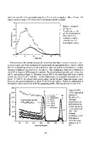
RESULTS AND DISCUSSION Implanted defect profiles versus Ge dose Figure 1 shows S parameter versus incident energy curves for samples implanted in the range lxlO0l - lxl0' 3cm-2 . The S parameters have been normalised to the value for undefected Si and hence tend to a value of 1 at high energies corresponding to depths beyond the implant range. The increase in S upto energies of 10keV corresponds to positron trapping at defects induced by the Ge implantation.
80
The data have been fitted using the program POSTRAP[9] assuming a positron trapping rate of lxlO"'s- and a specific defect S parameter value of 1.04; both typical of ion irradiation induced defects in Si [4]. The fits are shown as solid lines. The data can be adequately fitted by varying the concentration of defects contained in a simple rectangular distribution extending to 350nm from the surface. This compares to a value of -80nm
Data Loading...