Directed self-assembly lithography for half-pitch sub-15 nm pattern fabrication process
- PDF / 1,476,518 Bytes
- 12 Pages / 612 x 792 pts (letter) Page_size
- 91 Downloads / 259 Views
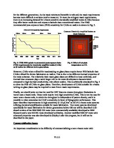
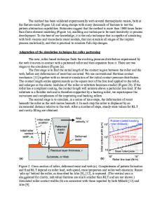
Directed self-assembly lithography for half-pitch sub-15 nm pattern fabrication process Hironobu Sato*1, Yuriko Seino1, Naoko Kihara1, Yusuke Kasahara1, Katsutoshi Kobayashi1, Katsuyoshi Kodera1, Hideki Kanai1, Yoshiaki Kawamonzen1, Shinya Minegishi1, Ken Miyagi1, Toshikatsu Tobana1, Noriyuki Hirayanagi1, Tomoharu Fujiwara1, Tsukasa Azuma1 and Teruaki Hayakawa2 1 EUVL Infrastructure Development Center, Inc., 16-1 Onogawa, Tsukuba, Ibaraki 305-8569, Japan 2 Tokyo Institute of Technology, 2-12-1-S8-26 Ookayama, Meguro, Tokyo 152-8552, Japan * Corresponding author: [email protected] ABSTRACT This paper introduces a fabrication method to achieve sub-15 nm line-and-space (L/S) patterns by combining grapho- and chemo-epitaxy using poly(styrene-block-methyl methacrylate) copolymer (PS-b-PMMA). The fabrication method is simple, since it eliminates photoresist stripping and also does not require any special materials to form pinning patterns. In this process, the ridges formed on spin-on-glass (SOG) surface work as physical guides and the photoresists on them are utilized as a pinning layer. Fine PS-b-PMMA L/S patterns were obtained in sufficient critical dimension (CD) range of the guide patterns that corresponded to the 15% dose margin using ArF immersion lithography. 3-dimensional grid defects were found to be the origin of the short defects. The half-pitch (hp) 15 nm L/S patterns were transferred successfully to SOG/spin-on-carbon (SOC) stacked substrate. We also describe fabrication of sub-10 nm L/S patterns using a high-chi block copolymer (BCP). INTRODUCTION Directed self-assembly (DSA) has recently been attracting semiconductor device manufacturers as a means of extending ArF immersion lithography. Several practical applications have been reported, such as contact hole shrink [1, 2] and tri-gate structure patterning for finFETs [3]. The PS-b-PMMA system is currently the most widely used material for obtaining L/S patterns around hp15 nm. Although there are several ways of achieving DSA patterning, pattern multiplication using chemoepitaxy seems to be the most promising candidate for high-volume manufacturing. Two patterning methods have been the subjects of much study, namely, LiNe flow [4] and SMARTTM [5] flow. A big difference between those two methods is the width of pinning line. The pinning width of the LiNe flow is 1/2Lo (Lo is BCP pitch), and that of the SMARTTM flow is 3/2Lo. Both require specific materials to form the pinning region. The LiNe flow uses cross-linkable PS (X-PS) to attract a PS segment of the PS-b-PMMA. On the other hand, the SMARTTM flow needs special grafting materials whose affinity is precisely controlled to attract a PS segment along with both sides of PMMA segments (or a PMMA segment along with both sides of PS segments) simultaneously. Both fabrication processes also require photoresist strip after reactive-ion etching (RIE). In the case of LiNe flow, photoresist is stripped after X-PS patterning using RIE. On the other hand, in the case of SMARTTM flow, photoresist should be st
Data Loading...