Effect of Buffer Layer and III/V Ratio on the Surface Morphology of Gan Grown by MBE
- PDF / 145,111 Bytes
- 6 Pages / 612 x 792 pts (letter) Page_size
- 51 Downloads / 327 Views
wnloaded from https://www.cambridge.org/core. IP address: 45.66.211.120, on 06 Jun 2020 at 06:49:33, subject to the Cambridge Core terms of use, available at https://www.cambridge.org/core/terms. https://doi.org/10.1557/S1092578300002829
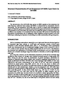
Figure 1: AFM micrographs of GaN grown on sapphire using GaN buffer layers. For nitrogen rich growth of the main layer (A) a rough surface and fine-grained microstructure results, while growth under slightly (B) and more heavily Ga-rich (C) conditions leads to larger grain size and flatter surfaces. The surface pictured in (C) is quite flat, with pit defects lying at the coalesced island boundaries. The vertical scale is 100 nm in these images.
growth was 8×10⁻⁵ torr. Effusion cells were used as sources of Ga, Al, and Si. The substrates were backside coated with Ti to assist in radiative heating, and were loaded into the vacuum system without chemical treatment. For each growth, the substrate was first heated to 800 °C and exposed to the nitrogen beam for 30 minutes at 450W RF power and at reduced nitrogen flow. Reflection high-energy electron diffraction (RHEED) patterns were bright streaks after the nitridation stage, indicating the formation of an AlN layer at the surface. A thin GaN or AlN buffer layer was then deposited at a nominal growth rate of 0.15 microns per hour at a plasma source power of 350W. For growth of GaN buffer layers, the III/V ratio was set close to unity, while for growth of AlN buffer layers the Al cell temperature was variably set to 1100 °C, 1120 °C, or 1130 °C representing N-rich, near stoichiometric, and Al-rich growth conditions, respectively. The growth time for the buffer layers was 2-3 minutes. After buffer layer deposition, the samples were soaked under the nitrogen beam for 8 minutes. The main GaN layer was then deposited at a rate of approximately 0.4 microns per hour. A series of samples was grown utilizing GaN buffer layers, wherein subsequent growth of the main layer was carried out under N-rich, slightly Ga-rich, or heavily Ga-rich conditions. For GaN layers grown on AlN buffer layers, flux conditions were slightly Ga-rich and constant. The total thickness of these layers was about 1 micron. Additionally, one sample was grown to a thickness of 2 microns using an AlN buffer layer. All films were doped with Si to approximately 1017 cm-3. The surface morphology of these layers was studied by atomic force microscopy in Tapping Mode using a Bioscope AFM with a Digital Instruments Nanoscope IIIa controller. RESULTS GaN buffer layers The surface morphology of GaN films is seen to depend strongly on the III/V ratio employed during RF plasma MBE growth. As has been previously observed [2-4], the RHEED image abruptly changes from spotty to streaky as flux conditions move from nitrogen-rich to gallium-rich. The surface morphology of films grown on GaN buffer layers and under various
Downloaded from https://www.cambridge.org/core. IP address: 45.66.211.120, on 06 Jun 2020 at 06:49:33, subject to the Cambridge Core terms of use, available at https://www
Data Loading...