Effect of Plasma Treatment on Crystallization Behavior of Amorphous Silicon Films
- PDF / 831,783 Bytes
- 6 Pages / 414.72 x 648 pts Page_size
- 0 Downloads / 286 Views
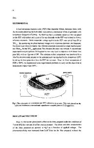
th of the reflectance peak at 276 nm is used as an indication of complete crystallization of the sample. For the selective crystallization experiments, SiO 2 deposited by e-beam evaporation and patterned by lithography and dilute hydrofluoric acid etched, was used as a mask during plasma exposure to realize polysilicon and amorphous silicon on the same substrate. EXPERIMENTAL RESULTS We have studied effect of hydrogen, oxygen and argon plasmas on the crystallization of a-Si:H. Hydrogen plasma has the largest effect, with the crystallization time reduced by a factor of five, and argon plasma had the smallest effect (figure 1). The change in reflectivity at 276 nm is used to monitor the degree of crystallization. The RF power was 200 W, pressure was 50 mtorr and flow rate 50 sccm. 8
6
5
o•
4 3
2
04
Annealing time at 600 0C (hrs) Figure 1. Change in UV reflectance at 276 nm as a function of annealing time for samples exposed to different plasmas.
The crystallization time, defined as the time taken to completely crystallize a-Si:H at 600 TC in N 2 ambient, falls as the RF power of the H2 or 02 plasma increases as in figure 2(a). In either case when the RF power is greater than 270 W, the plasma exposure leads to sputter I
16-
14-
t
-0-
150 nm a-Si:H deposited at 150 °C rf power = 200 W, pressure = 50 mton1 flow = 50 sccm
16-
Plasma exp osure time= 90 min ---
12E
150 nm a-Si:Hdeposited at 150 'C
14-
Hydrogen plasma Oxygen plasma
12-
E
10-
_-0- Hydrogen plasma
10.
-0-
0
0
80
64-
Oxygen plasma
8. 6.
I
4.
I C
20
40
80
80
100
120
140
180
180
200
Plasma exposure time (min)
RF Power (W)
Figure 2.Crystallization time of a-Si:H plasma treated samples as a function of (a) RF power and (b) exposure time. Pressure was 50 mtorr and flow-rate was 50 sccm.
578
etching of the film which can lead to pits and craters. The crystallization time also reduces as the plasma exposure time increases and saturates after 60 min exposure in case of H 2 and 180 min in case of 02 plasma exposure respectively, as illustrated in figure 2(b). The crystallization time also depends on the growth temperature of the a-Si:H films. It falls linearly from - 16 hrs to - 5 hrs for the untreated control sample as the growth temperature no treatment H2 plasma treated (200 W,90 min) 0 plasma treated (200 W. 90 min)
a-S:H on 7059 glass
18-
1616-
.
14A .~14.
- 14_E 4-
1210-
12 .0
10
1N0 200
0100 Deposition Temperature (°C)
20
300
30
40
Deposition Temperature (00)
Figure 3. (a) Hydrogen content in the a-Si film as a function of growth temperature, (b) Crystallization time for plasma treated and untreated samples as a function of growth temperature.
increases from 150 °C to 350 °C (figure 3(b)) and this correlates well with the hydrogen content (as measured by IR absorption at 630 cmt ) in the film, which also reduces linearly from ~16.9 to ~ 8.5 atomic % as the growth temperatures increases from 150 2Cto 350 °C (figure 3(a)). Oxygen plasma treated samples also show the same trend. But the hydrogen pla
Data Loading...