Effects of thermal annealing in the properties of PECVD a-SiC layers
- PDF / 194,433 Bytes
- 6 Pages / 612 x 792 pts (letter) Page_size
- 64 Downloads / 234 Views
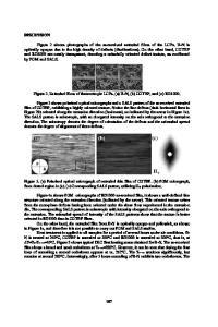
Effects of thermal annealing in the properties of PECVD a-SiC layers L.F. Marsal, J. Pallares, A. Orpella1, D. Bardés1, J. Puigdollers1 and R. Alcubilla1 Departament d'Enginyeria Electrònica. Universitat Rovira i Virgili, Tarragona, Spain. 1 Departament d'Enginyeria Electrònica. Campus Nord, Av. Gran Capita s/n. Mòdul C4. Universitat Politècnica de Catalunya, Barcelona, Spain. ABSTRACT Effects of thermal annealing in the properties of PECVD amorphous-Si0.8C0.2:H layers were studied. In order to reduce the density defects and increase the electrical conductivity, some samples were annealed: at 500 ºC during 1 hour followed by 15 minutes at 800 ºC. The results show that in the course of the thermal process, the hydrogen diffuse outside the film and the annealed Si0.8C0.2:H films tend to segregate in silicon clusters and, as a result, partially crystallize. Electrical dark conductivity shows an increase in more than six orders of magnitude, while the optical bandgap decreases from 1.9 eV to 1.4 eV. Annealed- Si0.8C0.2 films have been used as emitter in silicon bipolar transistors. Results indicate promising features such as low base currents and good emitter Gummel numbers. INTRODUCTION Hydrogenated amorphous silicon carbon alloys (a-Si1-xCx:H) deposited by Plasma Enhanced Chemical Vapour Deposition (PECVD) are of great interest because they can be deposited at relatively low temperature on large area, have a low cost of preparation, and are compatible with standard silicon technology. In addition, their optical bandgap can be modified from 1.7 to 3 eV by changing the carbon composition of the alloys. Between their applications some of them are of current interest: as a window material to enhance the conversion efficiency of solar cells [1], as a wide gap emitter in silicon heterojunction bipolar transistors (HBTs) [2], etc. However, amorphous silicon carbon alloys present a high density of states and a very low electrical dark conductivity, leading to high values of emitter resistance limiting the usefulness of the whole device. One way of circunvent these drawbacks is to formation of crystallites in the amorphous film. Nano or microcrystalline regions within the amorphous network increase the electrical conductivity and reduce the state density. Demichelis et al. demonstrated that microcrystalline Si1-xCx films can be produced under suitable conditions from SiH4 + CH4 mixtures with a high H2 dilution and high RF power density using PECVD or through annealing [3]. In another study, Wang et al. [4] also reported that crystallization of a-SiC films may be achieved by annealing treatments at temperatures between 800 and 1100 ºC. Another method to produce crystallization of a-SiC films is by excimer laser annealing [5]. In this context and despite of the large number of contributions on amorphous and annealing silicon-carbon films, the knowledge and comparability of the physical properties is difficult because they depend strongly on the preparation conditions and on the particular process used for deposition. In this wor
Data Loading...