Elastic Misfit Strain Relaxation in Highly Strained InAs Dots on GaAs as Studied by Tem, AFM and VFF Atomistic Calculati
- PDF / 1,750,461 Bytes
- 6 Pages / 414.72 x 648 pts Page_size
- 20 Downloads / 304 Views
results in the formation of islands in the Stranski-Krastanov growth mode. Transmission electron microscopy (TEM) studies of InGaAs on GaAs [9,10] or Ge on Si [11] have shown that at the early stages of formation, these islands may be free of dislocations and coherently strained to the substrate. In this paper, we report on the experimental TEM strain contrasts associated with such islands in plan-view samples (hereafter, the words quantum dots and islands will be used interchangeably). We also simulate images from dot strain fields determined either by continuous elastic models or by VFF calculations. The comparison between the observed TEM contrasts and computed images confirms the idea we have of such islands and thus provides experimental information on dot strain fields. EXPERIMENTAL InAs epilayers were grown by molecular beam epitaxy on a non intentionally doped 1 micrometer-thick GaAs buffer layer at 500'C and under an arsenic pressure of 6 x 10⁻⁶ Torr. The growth rate (0.06 monolayer s- 1) was calibrated by reflection high-energy electron diffraction (RHEED) oscillation measurements during InAs deposition, yielding a final approximate 2% accuracy for the coverage 0. The samples studied in the present work were obtained by interrupting the growth at the onset of the 2D-3D transition : they correspond to a threshold coverage 0 th = 1.75 monolayer (ML) for which spots (associated with the growth of 3D dots) suddenly appear on the RHEED diagrams [8]. The morphology of dots was determined with ex situ atomic force microscopy (AFM). Images were taken with various scanning directions and 569 Mat. Res. Soc. Symp. Proc. Vol. 355 01995 Materials Research Society
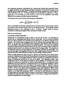
20' tip cantilevers, with similar results : the vertical resolution is better than 0.3 nm and the lateral resolution is better than 3 nm. For the preparation of plan-view TEM thin foils, the samples were mechanichally thinned approximately to 30 gtm from the substrate side and then ion-milled. TEM studies were performed with a Philips CM30 microscope operated at 300 kV. The [001] direction was chosen to be perpendicular to the interface plane and directed towards the epilayer side (islands on the top surface of the thin foil) (figure 1).
f
J
[001] •N
--a&- Epilayer .,91.."side).
Figure 1 : Schematic view of the InAs/GaAs thinned samples showing the conditions of observation in the electron microscope (the samples were thinned from the substrate
Substrate The simulated TEM images were performed with a program based on the resolution of the HowieWhelan equations [12] using the fourth order Runge-Kutta method originally employed by Head [13]. The strain field used to carry out the contrast simulations was either deduced from continuous elastic models or determined by VFF atomistic calculations. Continuous elastic models are limited to the case of elastic strain induced by sinusoidal or cycloidal fluctuations of a constrained thin film surface [14-16]. They have the advantage of introducing simple analytical functions (with a few adjustable parameters) in
Data Loading...