Electrical Properties of Nanoscale TiSi 2 Islands on Si
- PDF / 792,168 Bytes
- 6 Pages / 417.6 x 639 pts Page_size
- 63 Downloads / 402 Views
111 Mat. Res. Soc. Symp. Proc. Vol. 583 © 2000 Materials Research Society
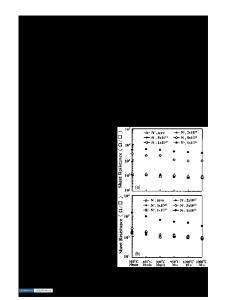
In previous studies, the SET effects were observed in a double-barrier junction structure prepared by tip/Au cluster/self-assembled monolayer of dithiol molecules on Au substrate[4]. Au cluster size was found to range between 5 and 10 nm. Other small metal clusters (less than 10 nm) such as gold [5], silver [6] or platinum [7] were deposited on the insulator/substrate forming well established double-barrier junction structures and showed single electron tunneling effects. Also a field evaporation of tip was used to deposit gold island on silicon by applying a short pulse between the gold STM tip and silicon substrate [8]. In this case the tunnel barrier is formed by the Schottky barrier formation between the metal island and the semiconductor substrate. We have introduced silicide nanoscale islands fabrication earlier, but, to our knowledge, there has been no reported work on charging effects of silicide nanoscale islands[9]. Our previous studies have shown that a thin layer of titanium reacts with the silicon substrate to form nanometer scale silicide island structures [10]. We suggest that these islands could prove to be suitable to display single electron charging. Our STM
measurements indicate that the dimensions of the TiSi 2 that can be -10 run, which is small enough to anticipate the occurrence of single electron charging effects. In this work, STS experiments were performed after forming TiSi 2 in situ on a Si(1 11)7x7 surface. The room temperature I/V measurements of these islands indicate Coulomb blockade and Coulomb staircases effects on these islands. EXPERIMENT The experimental setup consists of an ultra high vacuum system (base pressure < 4 x 10¹¹ Torr) with a commercial STM (Park Scientific, AutoProbe VP), AES, LEED, and an e-beam evaporator. A load-lock is used for sample introduction without breaking vacuum. A magnetically coupled transfer mechanism is used for sample movement and tip exchange. The whole system rests on an air table for vibration reduction during STM scanning. The substrate was P-doped, n-type (111) silicon having a resistivity of 0.1 Qcm. The sample was scribed into rectangles of 0.5 cmx 1.5 cm and then loaded onto the sample holder. The sample was heated resistively. After several hours of outgassing at 600 'C, the sample was flashed at 1200 'C for 30 sec. The temperature was measured with an optical pyrometer. Care was taken to keep the chamber pressure below 2x 10⁻⁹ Torr during the flashing. The flashing was repeated as necessary. The reconstructed 7x7 surface, confirmed by LEED, was achieved after the heat cleaning, and was used as a starting surface for the subsequent titanium deposition. Titanium was deposited at room temperature by electron beam evaporation of 99.9% pure titanium. The deposition rate was measured using a quartz crystal monitor. The nominal deposition rate used for this study was 0.2nm/min for thicknesses varying from 1 to 2 monolayers. Auger spectra were obtained after the depositio
Data Loading...