Electroluminescence Device Perspectives Of Si + -Implanted SiO 2
- PDF / 333,162 Bytes
- 6 Pages / 414.72 x 648 pts Page_size
- 48 Downloads / 292 Views
ABSTRACT
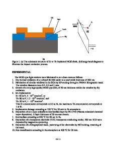
Thermal oxide layers on Si which have been implanted with Si conduct electrical current and emit light. The electroluminescence effect (EL) has an efficiency which is comparable to the best values that have been reported for the porous Si based devices. Generally, the EL spectrum differs substantially from the photoexcited luminescence. It is linked with that excited by external high energy electrons in cathodoluminescence (CL) experiments. We suggest to consider the effect as internal CL. Based on studies of transport and EL characteristic we evaluate the possibilities of an electroluminescent device based on such layers. INTRODUCTION The newest addition to the various schemes for preparing a system of photoluminescing nanoparticles is Si implantation into a thermal SiO 2 layer [1-4]. In contrast to electrochemical etching (porous Si) and gas-phase deposition (CVD particles), this yields a compact and closed layer. The particle size is controlled in a thermal precipitation step by varying the length of time and the temperature. The implantation technique affords precise dose and depth control. It is a processing technology that is an accepted tool in the manufacturing of electronic devices. The photoluminescence is tunable in the visible range [4-6] and has an efficiency comparable to that of porous silicon (PoSi) in its red-orange range of color. The implanted layers have an electrical conductivity that depends on the implantation dose and annealing treatments. The SiO,, material that forms the layer is related to the CVDSystem studied by DiMaria et al. [7] for its electroluminescence properties. All of these considerations suggest that one explore the prospect of an electroluminescent device based on electrical current passing through the thin nonstoichiometric SiOx covering the surface of the wafer. We report here on our experience with electroluminescence and discuss the problems and prospects encountered in trying to make light-emitting devices from such implanted oxide layers. SAMPLE PREPARATION Thermally grown Si-oxide, 100 nm thick on a (100) Si-wafer was implanted with Si' ions with an energy of 50 keV, and a dose of 5x1016 cm" 2 . The Si-substrate was either of p- or n-type. The implantation energy was chosen so that the highest Si density lies in the middle of the oxide layers. Afterwards the samples were annealed in a range of temperatures (300 - 1150 0C) for a time between 2 and 40 minutes in the nonoxidizing atmosphere of forming gas (H2 / N2). The implanted side was covered with several 4x4 mm pads of thin semitransparent Au films (- 100
A).
657
Mat. Res. Soc. Symp. Proc. Vol. 452 0 1997 Materials Research Society
PHOTOLUMINESCENCE INVESTIGATIONS The samples are studied using a prism spectrometer with a Si-diode detector or photomultiplier. The excitation source is a HeCd laser operating at 325 nm. The results depend sensitively on the annealing history and implantation dose of the sample. In Fig. 1 we summarize our observation for a few representative examples.
Wavelength (nm) 1000
Data Loading...