Electron Overflow to the AlGaN p-Cladding Layer in InGaN/GaN/AlGaN MQW Laser Diodes
- PDF / 133,453 Bytes
- 5 Pages / 612 x 792 pts (letter) Page_size
- 39 Downloads / 304 Views
Internet Journal Nitride Semiconductor Research
Electron Overflow to the AlGaN p-Cladding Layer in InGaN/GaN/AlGaN MQW Laser Diodes Kay Domen 1, Reiko Soejima1, Akito Kuramata 1 and Toshiyuki Tanahashi1 1Fujitsu
Laboratories Ltd.,
(Received Wednesday, December 24, 1997; accepted Thursday, January 29, 1998)
Current flow through an InGaN/GaN/AlGaN multi-quantum well (MQW) laser diode is simulated. We found that electron overflow to the AlGaN p-cladding layer is very large, which prevents the current injection into the MQW layers. We clarified that the electron overflow occurs easily in nitride lasers because of three intrinsic reasons; poor hole injection due to the small hole mobility and thermal velocity, the small conduction band offset for InGaN/GaN, and the high threshold carrier density. We show that the Al composition and the p-doping of the AlGaN p-cladding layer is of critical importance to obtain laser oscillation by current injection.
1
Introduction
Nakamura et al. reported 10,000 hours continuous-wave operation of nitride lasers [1] indicating that the laser is the most promising for the short-wavelength light source of the large capacity optical storages. However, it took 6 years to achieve laser diodes [2] after lasing by optical pumping at room temperature was first reported in 1990 [3]. This implies that some key issues underlying current injection have not yet been sufficiently clarified. Considering that it also took 3 years from the first commercialization of the nitride LED [4], the population inversion of carriers seems difficult for the nitride lasers. It is well known that the p-type doping has played an important role in the history of the nitride research [5] and the following realization of light emitting diodes (LED) [4]. High resistivity in p-cladding layers is still a matter of concern to nitride researchers. The hole injection then seems to be a problem. Another unclarified issue is the band-offset for the heterojunctions. The value for the band offset is very controversial. The valence band offset for InN/GaN has been reported to be theoretically 0.51 eV by Albanesi et al. [6], 0.48 eV by Wei et al. [7], and experimentally 1.05 eV by Martin et al. [8]. We believe that the conduction band offset for InGaN/GaN is small, based on the following observations [9]: we compared two LEDs and In0.07Ga0.93N/ with In0.13Ga0.87N/GaN Al0.05Ga0.95N double-hetero structures, both of which have the same bandgap difference between the active and the cladding layer. On current injection, the InGaN/
GaN LED showed a weak active layer luminescence and relatively strong deep-level luminescence in the GaN pcladding layer. These results indicated that the electron overflow to the p-cladding layer disturbs the current injection to the active layer. In contrast, the InGaN/ AlGaN showed strong active-layer luminescence. Since photoluminescence intensities were comparable for the two structures, we believe the conduction band offset is smaller for InGaN/GaN than for InGaN/AlGaN. The value for the ratio of
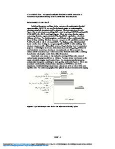
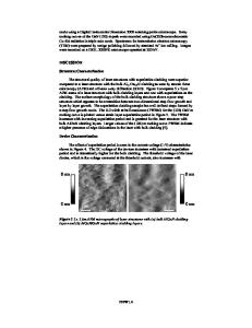
Data Loading...