Electronic Structure of Divalent Defects in Tetrahedrally Bonded Amorphous Materials
- PDF / 532,684 Bytes
- 6 Pages / 420.48 x 639 pts Page_size
- 4 Downloads / 343 Views
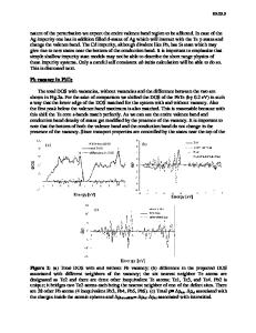
ELECTRONIC STRUCTURE OF DIVALENT DEFECTS IN TETRAHEDRALLY BONDED AMORPHOUS MATERIALS S.Y. LIN, G. LUCOVSKY, S. GUHA* and J.S. PAYSON* Department of Physics, N.C. State University, Raleigh N.C. 27965-8202 *Energy Conversion Devices, Inc., Troy, ML 48084 ABSTRACT This paper describes a calculation of twofold-coordinated (or divalent) intrinsic bonding defects in a-SiSn:H alloy films. The motivation for this study comes from experimental studies of the electronic and optical properties of aSi,Sn:H alloys which indicate dramatic changes in the electronic and photoelectronic properties for small concentrations of Sn (approximately 1-2 at. %). We have used a cluster Bethe lattice structural model and an empirical tight-binding Hamiltonian to investigate the electronic properties of tetrahedrally bonded Sn atoms and neutral Sn defect centers (T 2 and T30) and in an a-Si host. We find that: (C) fourfoldcoordinated Sn atoms simply promote a reduction in the optical bandgap, with the energy gap disappearing for Sn concentrations of about 20 to 30 at. %; (2) neutral dangling bonds (T *) or threefold-coordinated Sn atoms generate a localized state in the gap that is iower in energy than the corresponding neutral Si atom dangling bond; and (3) divalent (T 2 0) or twofold-coordinated Sn atoms give rise to two states in the gap, an occupied state that is lower in energy that either the Sn or Si dangling bond, and an empty state that is just below the conduction band edge. We show that the electronic and optical properties of the a-SiSn:H alloys can be understood in terms of a model in which there are relatively high densities of unhydrogenated Sn divalent sites and/or Sn dangling bonds. I INTRODUCTION There have been a number of studies of the optical and electronic properties of a-SiSn:H alloy films [1,2]. The motivation to study this system derives from a more general interest to tailor the band-gap of a-Si based alloys for specific device applications. In this instance the primary driving force has been in reducing the band-gap from an approximate value of 1.8-1.9 eV in a-Si*H (or a-Si-H:F) to about 1.4 eV in alloys intended for photovoltaic devices. Alloys of a-SiGe:H and aSiGe:H:F require approximately 50 at. Z Ge to reduce the band-gap to about 1.4 eV. This level of Ge atom alloying is generally accompanied by a significant decrease in the photoconductivity and luminescence relative to a-Si:H [3-5], and a related decrease in the performance of the intrinsic alloy materials in photovoltaic device structures. This degradation is not completely understood and may derive in part, or totally from any one of the following: (a) an increase in the number of deep localized states, a large fraction of which are Ge dangling bonds; (b) inadequate inhomogeneity of Ge sites relative to Si sites; this in manifest in preferential attachment ratios [(SiH/Si)/(GeH/Ge)] which range from 2 to 4 in magnetron sputtered films [4] to 20 in glow discharge deposited films [3]; and (c) to increases in film inhomogeniety, e.g., a microstructure that d
Data Loading...