Evidence for a defect-assisted low resistive conductivity in cw laser beam mixed Au/Te/Au/GaAs contacts
- PDF / 369,102 Bytes
- 6 Pages / 420.48 x 639 pts Page_size
- 52 Downloads / 225 Views
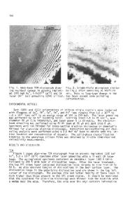
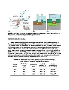
Evidence for a defect-assisted low resistive conductivity in cw laser beam mixed Au/Te/Au/GaAs contacts. J. Wattd*, R.E. Silverans*, H. Miinder*, and K. Wuyts*'* *Laboratorium voor Vaste Stof-Fysika en Magnetisme, K.U. Leuven, Celestijnenlaan 200D, B-3001 Leuven, Belgium **Institut fair Schicht-und lonentechnik, KFA Jillich, Postfach 1913, 5170 Jilich, Germany **Instituut voor Kern-en Stralingsfysika, K.U. Leuven, Celestijnenlaan 200 D, B-3001 Leuyen, Belgium Abstract CW laser beam mixed Au/Te/Au/n-GaAs contacts have been studied by RBS, M6ssbauer and Raman spectroscopy. For both low and high laser power mixing, resulting in respectively Schottky-type and ohmic contacts, the formation of non-uniformly dispersed Ga 2 Te3 crystallites was observed. However, for the ohmic contacts the formation of a high density of defect complexes in the GaAs surface layers was revealed. The experimental results suggest that the ohmic conduction mechanism is based on a hopping or a defect assisted tunneling process through the contact zone, consistent with the amorphous/highly defective heterojunction model. Introduction. Laserprocessing of metal/semiconductor contacts provides an attractive alternative for the conventional alloying in rapid time anneal systems. The main technological advantage of laser beam mixing lies in the ability to heat localized areas while the bulk wafer is kept at room temperature. The fast heating in a very short time interval (ranging from 10-6-10-s for pulsed mixing to 10-2_10-4S for scanned cw mixing) may however result in the formation of new and metastable phases[l/. On the other hand, the rapid freezing of dopants can give rise to dopant concentrations which can far exceed the solubility limit[2]. Furthermore, laser beam mixing is also known to cause deep levels in the substrate surface region[3]. Accordingly, a better understanding of the role of the defects in modifying the electronic behavior of the contacts is aimed. In our earlier study of pulsed laser beam mixed Au/Te/Au/GaAs contacts the observed low resistive conductivity was found to be correlated to the presence of a high concentration of Te-related defects in the contact zone[4]. To extend the study of the role of defects in laser beam mixed ohmic contacts an investigation of cw laser beam mixed identical contacts is presented in this paper. The main question about the nature of these structures is whether the low contact resistances can be explained by the formation of an amorphous/highly defective or a graded crystalline heterojunction or by the formation of a n+-doped GaAs surface. The observed low resistive conductivity is discussed in the light of the different competing models proposed[5/. Experimental procedures. 17 Metallization of the n-GaAs substrates, uniformly Si-doped to a dose of 3x10 at/cm was performed by succesive deposition of 50 A Au, 500 A Te and 1200 A Au on (100) oriented GaAs by resistive heating evaporation in vacua of the order of 10' Torr. The electrical measurements were performed on patterned wafers prepared by p
Data Loading...