Experimental Study of Sputter Deposited Contacts to Gallium Nitride
- PDF / 892,043 Bytes
- 6 Pages / 414.72 x 648 pts Page_size
- 65 Downloads / 391 Views
as pre-annealing[1], RIE processing[2], or ion implantation[3]. Laser diodes have also been successfully fabricated using these contacts as n- electrodes[4]. There has been considerable speculation about the exact role played by Ti in the formation of these contacts. It is believed that a thin (- 200 A) layer of Ti aids in reduction of the native oxide of GaN to facilitate Al contact to the fresh surface.[5] Also proposed is the formation of a TiN layer at the interface which results in N vacancies near the surface of GaN and thus locally high donor concentration. [6] Power- and high temperature devices require contacts that are thermally and chemically stable, and refractory metals such as tungsten have been studied as initial candidates for these applications. It is our hope here to elucidate on these issues from the viewpoint of sputtering surface treatments, as well as to explore the parameter space of metal type and interface preparation rather than attempt the achievement of ultra low values of
R,. We have conducted a sweeping study of various metal contacts to GaN, including Al, TiAl, Cr, Mo, W, Au, Sb, Ce, and Mg, which were applied with varying surface sputtering treatment techniques. Many of these metals were found to result in linear or almost linear pad-to-pad current-voltage characteristics, and for these, specific contact resistance was measured by the circular transmission line method (CTLM) [7)[8]. For those metals that produced highly rectifying contacts, the Schottky barrier heights and ideality factors were measured. 1089 Mat. Res. Soc. Symp. Proc. Vol. 482 01998 Materials Research Society
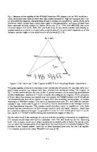
d Figure 1: Schematic diagram of the circular contact layout used for contact resistance measurements. The outer radius R1 is fixed at 200 pm. The inner contact radius varies so that the gap spacing d is 50, 30, 20, 15, 10, and 5 im. EXPERIMENT
Gallium nitride was grown by molecular beam epitaxy (MBE) on c-plane sapphire substrates employing a low temperature (650 'C) AIN buffer layer. The backs of the substrates were coated with Mo to facilitate radiative heating, and substrate temperature was held at 800 'C during growth under slightly metal-rich conditions. The growth rate was 0.35 pm/h and the final film thickness was nominally 1 Am. Two types of samples were studied that differed in electron concentration. High resistivity samples were unintentionally doped to approximately 1015 cm- 3 as measured by Van der Pauw Hall technique, and lower resistivity samples were doped by coevaporation of Si during growth to n = 9.2 - 101"cm- 3 . Although more highly doped material is expected to produce less resistive contacts, the more insulating samples focused on here were used to render a large degree of differentiation in contact properties caused by various sample preparations. Contact samples were prepared by cleaning the GaN films in organic solvents and by HF:H 20 2 solution which removed the backside metallization from the sapphire substrates. Metals under study were deposited and patterned by liftoff photoli
Data Loading...