Exploration of the Ultimate Patterning Potential Achievable with Focused Ion Beams
- PDF / 1,062,561 Bytes
- 10 Pages / 612 x 792 pts (letter) Page_size
- 25 Downloads / 334 Views
1089-Y03-01
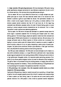
Exploration of the Ultimate Patterning Potential Achievable with Focused Ion Beams Jacques Gierak1, Eric Bourhis1, Dominique Mailly1, Gilles Patriarche1, Ali Madouri1, Ralf Jede2, Sven Bauerdick2, lars bruchhaus2, Peter Hawkes3, Anne-Laure Biance4, Birgitta Schiedt4, Loïc Auvray4, Laurent Bardotti5, Brigitte Prevel5, Pascal Mélinon5, Alain Perez5, Jacques Ferré6, Jean Pierre Jamet6, Alexandra Mougin6, Claude Chappert7, Véronique Mathet7, Lionel Aigouy8, Isabelle Robert-Philip1, Isabelle Sagnes1, Rémy Braive1, Alexios Beveratos1, and Izo Abram1 1 LPN, CNRS, Route de Nozay, Marcoussis, 91460, France 2 Raith GmbH, Hauert 18, Technologiepark, Dortmund, 44227, Germany 3 CEMES/CNRS, 29 rue Jeanne Marvig, Toulouse, 31055, France 4 MPI, Université d’Évry Val d’Essonne, Bd. François Mitterrand, Évry, 91025, France 5 LPMCN, UCB Lyon I et CNRS, 43 Bd du 11 Novembre 1918, Villeurbanne, 69622, France 6 LPS, UMR CNRS 8502 Univ. Paris Sud, Bâtiment 510, Orsay, 91405, France 7 IEF, Université Paris-Sud, Bât 220, Orsay, 91405, France 8 ESPCI, CNRS UPR 5, 10 rue Vauquelin, Paris, 75231, France ABSTRACT In this work we aim at evaluating the nano-structuring potential of a highly Focused Ion Beam. We will first detail a very high resolution FIB instrument we have developed. Then we will introduce and illustrate some advanced FIB processing schemes explored with this instrument. These patterning schemes are (i) Artificial nanopores direct engraving. (ii) Local defect injection for magnetic thin film direct patterning. (iii) Functionalization of atomically clean graphite surfaces. (iv) Engineering of the optical properties of microcavities. INTRODUCTION Progresses in nanosciences and nanotechnologies are intimately related to the development of imaging and patterning tools allowing either the “bottom up” approach, (STM, AFM, pulsed tip writing, local oxidation, ink jet, etc.) [1] or in continuing to advance the ultra-sophisticated nanolithography equipment (EBL, FIB, …), that make it possible to directly “paint” complex patterns on substrates. This hands-on approach can be contrasted with “Self-assembly” which attempts to take nature as a model and assemble complex structures from the starting point of interacting molecules or other nano-objects. With respect to this, ion beams are well suited to nano-fabrication and have long been used to modify the topography and the electronic properties of materials by etching, doping, or local deposition leading to the very popular Focused Ion Beam (FIB) technique. Historically the FIB developments was started in the late 70s [2] and nowadays FIB systems are intensively used in many industrial or academic research labs. Existing FIB technology almost exclusively uses gallium ions and enables localized milling and deposition of conductors and insulators with high precision [3] and hence its success in device modification, mask repair, process control, failure analysis [4, 5, 6].
14
30000
12
25000
10
Probe current (pA)
Tip emission voltage (V)
35000
20000 15000 10000 5000
8 6 4
Data Loading...