GaN Quantum Dots Grown at High Temperatures by Molecular Beam Epitaxy
- PDF / 451,125 Bytes
- 6 Pages / 595 x 842 pts (A4) Page_size
- 68 Downloads / 368 Views
E2.4.1
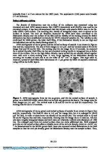
GaN Quantum Dots Grown at High Temperatures by Molecular Beam Epitaxy Tao Xu, Adrian Williams, Christos Thomidis and Theodore D. Moustakas Dept. of Electrical and Computer Engineering, Boston University, Boston, MA Lin Zhou and David J. Smith Dept. of Physics and Astronomy and Center for Solid State Science, Arizona State University, Tempe, AZ ABSTRACT In this paper we report the growth by MBE of GaN quantum dot superlattices (QDSLs) with AlN barriers on (0001) sapphire substrates at relatively high temperatures (770 oC) by the modified Stranski-Krastanov method. TEM studies indicate that the GaN QDs are truncated pyramids. We find that the height distribution of the dots depends strongly on the number of GaN monolayer coverage on the top of AlN. Specifically, we find that the height distribution consists of two Gaussian distributions (bimodal) for coverage of 3 and 4 MLs, and becomes single Gaussian distribution for 5 and 6 MLs of coverage. Furthermore, we find that the density of quantum dots increases with the degree of coverage and saturates at 2x10¹¹ dots/cm2. The number of stacks in the superlattice structure was also found to lead to bimodal height distribution of the QDs. Ordering of the quantum dots was accomplished by thermal annealing of the sapphire substrates at 1400 oC prior to the growth of GaN QDs. The annealing process reveals the vicinal steps due to the miscut of the substrates and the GaN QDs were found to line up along those steps. Photoluminescence studies show a broad luminescence spectrum centered at 3 eV which is red shifted with respect to that of bulk GaN and is consistent with internal fields due to polarization (Quantum Confined Stark Effect). Furthermore, we find that the luminescence intensity increases with the number of stacks in the superlattice structure due to higher spatial density of QDs. INTRODUCTION Quantum dots (QDs) can be used as the active region of opto-electronic devices, such as LEDs, lasers, modulators, and detectors. The challenges in the growth of GaN QDs lie in the development of methods to obtain dots with good size uniformity and high spatial density. Recently, there has been significant progress in control of GaN QD growth using StranskiKrastanov mode by MBE [1-4]. Adelmann et al.[1] studied the GaN QD growth under N-rich conditions at 730 oC. Under these conditions, QDs are formed in the presence of N2-plasma. The GaN QD growth was also studied under Ga-rich conditions, which was referred as “modified SK mode” [2, 3]. The 2D GaN film grown on AlN under Ga-rich conditions is spontaneously rearranged into 3D islands when allowing the excess Ga to desorb under vacuum. Furthermore, it has been reported [1] that the GaN QD density often saturates at about 1011 dots/cm2. GaN QD superlattices (SLs) can be used to increase the spatial density in the vertical direction. GaN optoelectronic devices are usually grown by MBE at 750-800 oC. However, for most of the results reported in the literature, the growth temperature for GaN QDs is 650 – 750 oC. In order to appl
Data Loading...