High Doped p-Type GaN Grown by Alternative Co-Doping Technique
- PDF / 150,760 Bytes
- 7 Pages / 595 x 842 pts (A4) Page_size
- 101 Downloads / 297 Views
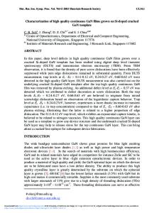
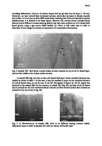
High Doped p-Type GaN Grown by Alternative Co-Doping Technique Souhachi Iwai, Hideki Hirayama and Yoshinobu Aoyagi Semiconductors Lab., RIKEN (The Institute of Physical and Chemical Research) , Hirosawa, Wako-shi, Saitama 351-0198, JAPAN ABSTRACT We investigated the electrical properties of Mg-doped GaN grown by alternative pulse supplies of source and dopant materials in metalorganic vapor phase epitaxy. We obtained the hole concentration of 6x1018cm-3 for p-type GaN grown on a sapphire substrate by repetition of supply and purging of Ga and Mg sources in the constant NH3 flow, while that of p-type GaN grown by the constant feeding of Ga and Mg sources was 2x1018cm-3. By using alternative feedings of Ga source and NH3 with Mg-Si co-doping, we obtained a highly hole concentration of 2x1019cm-3 for p-type GaN which was grown directly on a low temperature AlN buffer layer. We also obtained the hole concentration of 6x1018cm-3 for p-type GaN which was grown on an AlGaN layer on a SiC substrate by alternative co-doping technique. The activation energies for Mg-doped GaN grown by the pulse feedings of source materials were lower than that for GaN grown by continuous supplies of source materials as used in the conventional technique. INTRODUCTION Realization of highly conductive p-type GaN and AlGaN is essentially important for optical and electrical devices using nitride compounds. High conductive p-type cladding and contact layers are necessary for ultraviolet light emitting diodes (LEDs) and laser diodes (LDs). For wide-bandgap semiconductors, it is difficult to realize high conductivity p-type layer because of the large activation energy of acceptor impurities. Co-doping is theoretically proposed to get high hole concentration in p-type GaN and AlGaN [1]. According to the previously reported theory, donor and acceptor impurities are doped simultaneously and acceptor-donor-acceptor complexes are formed. In this case, compensation should be avoided and the activation energy of acceptor should be reduced by the formation of complexes. Codoping in GaN has been reported.[2-6]. However, it is difficult to get highly doped p-type GaN by conventional co-doping technique. If p-type and n-type impurities are supplied at the same time in continuous feeding of source materials, donor and acceptor atoms will be distributed randomly in the crystal and compensation is supposed to occur. In this paper, application of atomic layer epitaxy (ALE) is proposed for doping two impurity atoms in the desired configuration. In ALE growth of GaN, source materials are fed alternatively into a reactor [7,8]. In our study, p-type GaN layers are grown by two different techniques in which pulse supplies of source and dopant materials are performed in a low pressure metalorganic vapor phase epitaxy (MOVPE). Hole concentrations of p-type GaN layers are compared with Mg-doped GaN grown by continuous supplies of source materials as used in conventional growth technique. The activation energies are also compared with that of Mg in GaN grown by convention
Data Loading...