High Sensitive Strain Microsensor based on Dielectric Matrix with Metal Nanoparticles
- PDF / 192,093 Bytes
- 5 Pages / 414.72 x 648 pts Page_size
- 13 Downloads / 254 Views
ABSTRACT A dielectric matrix, containing metal nanoparticles with interparticle spacings of 1-2 nm, is a system with tunnel mechanism of electrical conductivity. Its electrical resistance is very sensitive to deforming of matrix because it leads to changes in spaces between particles and as a result the potential barrier transperancy is varied. Different metals (Mo, Cr, Ta, Au, Pt, Bi, Al) and their films morphology structure were studied in order to get high sensitive strain sensors. Metal nanoparticles were deposited on elastic dielectric substrates. Strain coefficients were measured for a wide range of strains and temperatures. Variation of matrix structure gives possibilities to produce strain sensors with high electrical resistance and weak temperature dependence. The matrix with Au nanoparticles was found to have maximum strain coefficient (>100 ). These sensors can be manufactured in the miniature scale (sensitive area around 1 micron or less). INTRODUCTION Discontinuous metal films represent a system of nanoscale islands on dielectric substrate. They are formed at early stages of vacuum deposition of metals on nonwettable substrates. Conductivity in such films is provided by electron tunneling. It is usually modeled as a system of potential wells and barriers. Thus, the conductivity is very sensitive to the distances between metal islands [1]. When an island metal film is deposited on an elastic substrate , then bending can effectively change the distances between islands (e.g. tunnel barrier width). This causes essential changes in film resistance. Resistance in such system is determined as [2]:
R = Aa 2 exp(47ta/h)(2m* H) 1/2 exp AE/kT,
(1)
where A - constant, a - distance between islands, h - Planck's constant, m* - effective mass of the tunneling electron, H - tunnel barrier height, AE - activation energy, k - Boltzmann's constant, T - absolute temperature When current passes through an island film, the phenomena of electron and light emission are observed in island metal films under certain conditions [3]. Conducted experiments showed high sensitivity of the electron emission current to substrate deformation. EXPERIMENT Island metal films were deposited by vacuum evaporation ( residual gas pressure P during vaporizing was P=2 10-4 Pa. Steel foils covered by dielectric layer were used 261
Mat. Res. Soc. Symp. Proc. Vol. 459 ©1997 Materials Research Society
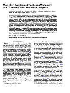
as elastic dielectric substrates. A pair of contacts in the form of thin (thickness of 0.2 ýtm) and narrow strips (width of 3 mm) were deposited on the substrate before island film deposition. The distance between contacts was equal 30 jtm (Fig.l)
__ 3
[
4 2
F-1
K~~F Fig.1. Sketch of the sample with island film and it's possible deformation: 1-elastic substrate, 2-dielectric layer, 3-electrical contact, 4-metal island. The thin film structure was studied by transmission electron microscopy. The particle size and the interparticle spacing were measured from the microscope photographs. The film structure was varied by using different conditio
Data Loading...