In Situ Optical Observation and Control of Initial Stages of GaAs Growth On Caf 2 Surface Modified by Electron Beam Irra
- PDF / 2,041,308 Bytes
- 6 Pages / 414.72 x 648 pts Page_size
- 55 Downloads / 251 Views
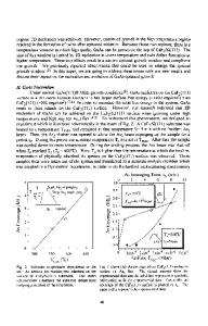
beam assist and group V atoms, As or P, supplied simultaneously occupied the surface F vacancy sites so as to improve wettability of over grown GaAs. Although the improvement of crystallinity of the GaAs layer grown by this technique was remarkable, the electrical properties of the layer have not been satisfactory compared to that of bulk crystal so far. In order to improve the film property, in situ observation of surface modification process and control of growth process are expected to be useful. However, it is difficult to observe the fluoride surface using electron diffraction method because the fluoride surface is very sensitive to electron beam irradiation and the beam effect can not be neglected. So we applied the surface photoabsorption (SPA) method [11] using a visible light which is expected not to affect the fluoride surface. Recently, we observed the surface modification process by the SPA method in which the sensitivity of the surface condition changes was increased by utilizing interference effects [12]. As a result, it was found that Ca colloids were generated on the CaF2 surface by low energy electron beam irradiation and that it could be suppressed when the surface modification was carried out using 300 eV electron beam at 200°C. In this work, the progress of the modification process and initial growth stage of GaAs were observed by means of SPA technique. And surface morphologies of GaAs grown on the modified CaF 2 surfaces were observed by atomic force microscopy (AFM) in order to comprehend the basis of surface modification effect. EXPERIMENT The experiment was carried out using a 3 chambers MBE system composed of a load lock and of two growth chambers for fluorides and for GaAs. After thermal cleaning of Si(1 11) 101 Mat. Res. Soc. Symp. Proc. Vol. 448 0 1997 Materials Research Society
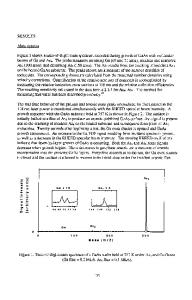
substrate at 900'C to obtain 7 X 7 superstructure in reflection electron diffraction pattern, 20 nm thick CaF2 films were grown on the substrate. Base pressure of fluoride growth chamber was less than 6X 10⁻⁹ torr and pressure during the growth was 1 X 10.- torr. After the substrate was transferred to the GaAs MBE growth chamber in which base pressure was less than 2X 10⁻⁹ torr, its surface was irradiated by an 300 eV electron beam at 200°C using an electron gun facing to the substrate under As 4 molecular beam impingement. After the surface modification process, GaAs growth was followed by opening a Ga cell shutter. The As 4 pressure during the electron beam irradiation and the GaAs growth was estimated as the equivalent pressure of the order of 10.5 torr at the sample surface. The surface modification and succeeding growth process was observed in situ by the SPA method as shown in Fig. 1. A p-polarized Ar ion laser light (488 nm) of which incident angle was set to 830 was employed as the probing light. The reflected light was detected by a Si photodiode and the output was lock-in amplified. The SPA signal was CaF2/Si(1 11) substrate taken as AR/R, where R is initial reflected intensity and AR is the variance
Data Loading...