Low-temperature electrical characteristics of the Au/Si interface
- PDF / 587,163 Bytes
- 5 Pages / 594 x 774 pts Page_size
- 31 Downloads / 301 Views
I.
INTRODUCTION
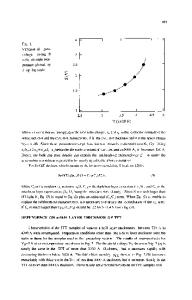
IN integrated circuit packaging, back-side contacts are required to be ohmic for a wide range of temperatures. Evaporated gold has been used to coat the back side of the die to achieve such contacts I and also to avoid the problem of chip cracking in its package resulting from temperature fluctuation of its environment. However, a number of gold-coated p-type silicon substrate products have failed to exhibit ohmic behavior at low temperatures. Rectifying contacts are observed in the temperature range from - 5 0 °C to 0 °C with eutectic die-attached products. On the other hand, identical devices which are die-attached with polyimide exhibit ohmic behavior in the same range of temperature. To clarify this issue, a systematic investigation was conducted on the current-voltage (I-V) characteristics of different contact structures. Measurements of the Schottky junction barrier height as a function of temperature were performed. Effect of heat treatment on the electrical behavior was examined. Possible mechanisms responsible for the observed rectifying behavior at low temperatures were considered. Specimens with front-side A1 and back-side Au contacts were tested to verify further the validity of the proposed model. As a proposed solution to this problem, a method to improve the low-temperature behavior is demonstrated. II.
SPECIMEN PREPARATION
A p-type wafer identical to the one used for the actual NMOS product is coated on both sides with a 2000-angstrom layer of evaporated gold. This double-gold-coated test structure (DG) is alloyed (420 °C for 7 minutes) to provide
A. TRAN is Process Engineer, Siliconix Inc., Santa Clara, CA 95054, and part-time Graduate Student at Santa Clara University, CA 95053. C.Y. YANG, Associate Professor and Director, and M. GAO, Visiting Associate Professor, are with the Microelectronics Laboratory, Department of Electrical Engineering and Computer Science, Santa Clara University, CA 95053. N. KIM is Scientist, High Technology Center, Boeing Electronics Company, Seattle, WA 98124. R. F. COOLEY is Manager, Packaging and Assembly Technology, Siliconix Inc., Santa Clara, CA 95054. Manuscript submitted February 10, 1986.
METALLURGICALTRANSACTIONS A
a good metallurgical contact on both the front and back sides of the wafer. The wafer is then diced and bonded into ceramic packages using two different die-attach methods, polyimide and eutectic. The weight composition of the eutectic preform used is 98 pct gold and 2 pct silicon. The type of polyimide adhesive used contains 62 pct silver by weight. In the eutectic die-attach process j'2 the package is heated by a heater block to 420 °C for one minute. Next a piece of gold preform is placed on the package. The die is then positioned in the package cavity on top of the melted preform and is gently scrubbed until eutectic wetting around the die perimeter is visible. The package is then removed from the heater block and is allowed to cool to room temperature. The polyimide die-attach process 3 utilizes an automatic die bonder with
Data Loading...