Metal Organic Chemical Vapor Deposition Growth of GaN and GaMnN Multifunctional Nanostructures
- PDF / 164,925 Bytes
- 6 Pages / 612 x 792 pts (letter) Page_size
- 68 Downloads / 308 Views
0901-Ra13-04.1
Metal Organic Chemical Vapor Deposition Growth of GaN and GaMnN Multifunctional Nanostructures Shalini Gupta1, Hun Kang1, Matthew Kane1,3, William E. Fenwick1, Nola Li1, Martin Strassburg1,2, Ali Asghar1, Nikolaus Dietz 2, and Ian T. Ferguson1, 3, ∗ 1 Georgia Institute of Technology, Electrical and Computer Engineering, Atlanta, GA 30332, U.S.A. 2 Georgia State University, Department of Physics and Astronomy, Atlanta, GA 30303, U.S.A. 3 Georgia Institute of Technology, School of Materials Science and Engineering, Atlanta, GA 30332, U.S.A. Abstract Quantum dots (QDs) have been shown to improve the efficiency and optical properties of opto- electronic devices compared to two dimensional quantum wells in the active region. The formation of self-assembled GaN nanostructures on aluminum nitride (AlN) grown on sapphire substrates by Metal Organic Chemical Vapor deposition (MOCVD) was explored. This paper reports on the effect of in-situ activation in nitrogen atmosphere on MOCVD grown GaN nanostructures. The effect of introducing manganese in these nanostructures was also studied. Optically active nanostructures were successfully obtained. A blue shift is observed in the photoluminescence data with a decrease in nanostructure size. Introduction GaN and its alloys with InN and AlN have been used for optoelectronic devices with blue and green wavelengths [1, 2]. High dislocation densities are present in group III - nitride heterostructures which render it necessary to localize the carriers for light generation and prevent nonradiative transitions. Therefore, reducing the dislocation density, increasing the amount of localization sites for carriers, or both may contribute to improved efficiency of light emitting devices. One way to achieve this is incorporating zero dimensional quantum dots (QDs) instead of the two dimensional quantum wells as QDs provide three-dimensional (3D) carrier confinement [3]. Stranski-Krastanow (SK) -like growth mode is not supported for the lattice mismatch between GaN and AlN (~2.5%). According to the theoretical model developed by Daruka et al. [4] a 3D growth by a ripening process that creates large islands is predicted for GaN/AlN heterostructures based on kinetics and thermodynamics [5]. However, under extreme growth conditions GaN nanostructures have been shown to have SK-like mode formations on SiC substrates using Molecular Beam Epitaxy (MBE) and MOCVD [6, 7]. This paper presents the nucleation studies of GaN nanostructures on AlN grown on sapphire substrates by MOCVD. Further, an activation step is introduced to the GaN/AlN hetero-system to support the formation ∗
Corresponding author: Ian Ferguson. 778 Atlantic Drive, Atlanta, Ga 30332-0250
Fax: (404) 385-2886 E-mail:[email protected]
0901-Ra13-04.2
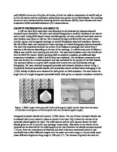
of 3D islands revealing a SK-like growth mode. Optically active GaN nanostructures were successfully obtained. Mn was incorporated into the GaN nanostructures to explore the growth conditions for ferromagnetic nanostructures. It has been shown in recent years that MOCVD
Data Loading...