Multiscale Modeling of Thin-Film Deposition: Applications to Si Device Processing
- PDF / 2,237,275 Bytes
- 8 Pages / 612 x 792 pts (letter) Page_size
- 109 Downloads / 307 Views
Multiscale Modeling of Thin-Film Deposition: Applications to Si Device Processing
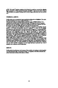
F.H. Baumann, D.L. Chopp, T. Díaz de la Rubia, G.H. Gilmer, J.E. Greene, H. Huang, S. Kodambaka, P. O’Sullivan, and I. Petrov Introduction Metallization is the back end of the integrated-circuit (IC) fabrication process where the transistor interconnections are formed. Figure 1 shows the metallized part of a static random-access memory chip. Metal lines for electrical connections (Al and Cu) in Si devices are deposited as blanket films and then etched or polished away to define the conducting lines. The deposition of insulating layers of materials such as SiO2 complete each vertical level of metallization. Barrier-layer films are deposited on the insulating layer to prevent the conducting metal from diffusing into or reacting with the insulating layers and ultimately to protect the electrically active Si regions (see Reference 1 for an excellent review of Al metallization technology). The back-end processing of ICs is becoming more complex as device components shrink in size and as the number of levels (now five or six) of metal conductors increases.2 The cost and the number of processing steps required for back-end metallization are now about equal to those for the complementary metal-oxide semiconductor (CMOS) transistors composing the front end of the device1 (see the June 2000 issue of MRS Bulletin for extensive discussions of front-end processing3). For this reason, predictive modeling is becoming an important tool for optimizing the reliability and integrity of interconnect structures.
182
Aluminum conductors are used in most Si devices currently4 (e.g., the AMD Athlon™ microprocessor), and a typical sequence of thin films is SiO2/Ti/TiN/Al. In this sequence, the Ti serves as a “glue” layer, providing better adherence to SiO2, while TiN is a diffusion barrier between SiO2 and Al. A cross-sectional transmis-
Figure 1. Scanning electron micrograph of an interconnect structure on a static random-access memory chip. The intermetal dielectrics are removed chemically for imaging purposes. Each metal layer requires three etching and seven deposition steps.
sion electron microscopy (TEM) image of a field-programmable gate array is shown in Figure 2. In this micrograph, the Ti and TiN layers are indistinguishable, and they correspond to the thin dark films below the Al metal lines. Tungsten plugs connecting the three layers of Al lines are clearly visible as the dark, tapered cylinders. The W is deposited by chemical vapor deposition (CVD), which provides good filling of the vias etched in the insulator. In order to cope with shrinking transistor size (gate widths approaching 100 nm), Cu metallization is currently being used in some microprocessors and other devices due to its lower resistivity (with concomitant reduction in RC signal delay), where device speeds are critical. A typical film stack in this case is SiO2/Ta/Cu, but the conducting Cu layer is usually deposited in two steps. A thin seed layer is first sputtered onto the b
Data Loading...