Nanoscale liquid phase epitaxy between Si and Au nanoparticles
- PDF / 569,874 Bytes
- 5 Pages / 612 x 792 pts (letter) Page_size
- 38 Downloads / 280 Views
MATERIALS RESEARCH
Welcome
Comments
Help
Nanoscale liquid phase epitaxy between Si and Au nanoparticles Yutaka Wakayama, Haruko Fujinuma, and Shun-ichiro Tanaka Tanaka Solid Junction Project, ERATO, Japan Science and Research Corporation, 1-1-1 Fukuura, Kanazawa-ku, Yokohama 236, Japan (Received 16 July 1997; accepted 26 September 1997)
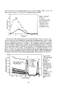
A self-assembly technique was used for fabrication of a Si/metal interface in nanometer scale. Fine particles of gold of nanometer-order diameter were generated by a gas-phase condensation method and deposited on a Si substrate. Through a heat treatment and a cooling process, a nanoscopic Si–Au composite structure was formed on the surface of the Si substrate. Then, surface diffusing Si atoms played an important role for fabrication of the Si–Au structure which were epitaxially grown projecting onto the substrate. Furthermore, the SiyAu interface was atomically flat with no mixed-layer formation, and the Au nanoparticles also had the same crystal orientation as that of the Si dots in spite of a large lattice constant mismatch between them. This structure was considered to be fabricated as a result of minimization of the total surface and interface energy of the SiyAu system.
I. INTRODUCTION
A new technique for fabrication of a heteromaterial junction in nanometer scale was investigated. By use of Au nanoparticles as a transport medium for liquid phase epitaxy (LPE), a dot-like structure of Si and Au was formed on the surface of a Si substrate. Here we describe the self-assembly process in which the SiyAu nanostructure is formed and the atomic-scale structure of this heteromaterial system. In recent years, advancing development of semiconductor devices has resulted in reduction of their elemental size. Realization of this improvement has involved much effort in lithographic techniques development.1–3 As a result, very fine patterning has been achieved, even to a submicron order. On the other hand, quantumsize devices have attracted much attention from the viewpoint of future VLSI technology.4–6 However, they are even less than 10 nm in size and beyond the scope of conventional lithographic techniques. Use of scanning probe microscopy is considered a possible means of overcoming this problem. For example, a scanning electron tunneling microscope (STM)7,8 and an atomic force microscope (AFM)9,10 have been used for fine patterning of metals on a semiconductor surface. Such techniques are very useful for site-selective patterning even on an atomic scale. A self-assembly technique for fabrication of quantum-size devices is also worth noting. Use of this technique has been investigated, especially for compound semiconductors using a self-assembly mechanism of these materials.11–14 On the other hand, the fabrication of a heteromaterial junction, for example, between a semiconductor and a metal, is essential for the development of quantum-size devices. 1492
http://journals.cambridge.org
J. Mater. Res., Vol. 13, No. 6, Jun 1998
Downloaded: 18 Mar 2015
In this work, we demonstrate t
Data Loading...