Non-contact Electrical Measurements of Sheet Resistance and Leakage Current Density for Ultra-shallow (and other) Juncti
- PDF / 2,256,431 Bytes
- 6 Pages / 612 x 792 pts (letter) Page_size
- 3 Downloads / 244 Views
C11.9.1
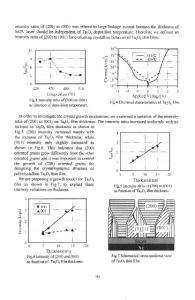
Non-contact Electrical Measurements of Sheet Resistance and Leakage Current Density for Ultra-shallow (and other) Junctions Vladimir N. Faifer, Michael I. Current, Wojtek Walecki, Vitali Souchkov, Georgy Mikhaylov, PhucVan, Tim Wong, Tan Nguyen, Jiansong Lu, S.H. Lau and Ann Koo Frontier Semiconductor, 1631 N. 1st Street, San Jose, CA 95112 USA, [email protected] ABSTRACT A novel, non-contact method for determination of ultra-shallow junction sheet resistance and leakage current density has been developed based on monitoring the dynamics of photo-generated carriers by means of spatially separated capacitive probes. At light modulation frequencies of about 100 kHz, spatially resolved surface voltage signals give a direct measure of the junction sheet resistance, independent of the junction depth. At lower light modulation frequencies, the junction leakage current density is determined. Combining capacitive monitoring of modulated photo-generated free carriers with a precision wafer motion stage allows for rapid acquisition of sheet resistance and leakage data for efficient wafer-scale mapping applications. SHALLOW JUNCTION SCALING With gate lengths of advanced CMOS logic devices scaling to 50 nm and less, the proportional scaling of source/drain extensions over the years 2003 to 2007 calls for junction depths of 25 nm and less and sheet resistances in the range from 200 to 900 Ohm/square [1]. The continued increase in chip transistor count (heading towards 109 per device) has driven a strong effort to understand and constrain the sources of leakage currents and other non-functional power drains. The increased impact of short channel effects for deeply scaled CMOS transistors indicate that tight process controls (of the order of 1% or less for dose and energy) are required for source/drain extension implants in order to maintain reasonable (5% range) controls on threshold voltage and other key transistor characteristics [2, 3]. At the same time, the predominant metrology for implant process control used over the last two decades, sheet resistance measurements with 4-point probes, encounters severe challenges due to physical and electrical punch through for junctions of 50 nm and less [4]. Even with the use of “soft”, non-penetrating probes, junction leakage currents continue to cause large errors in direct contact measurements due to mixing of current flows thorough the junction and into the subjunction layers. Optical interference and reflection methods give structural information on junction depth and damage density but have limited or no sensitivity to electrical activation of shallow junction dopants and do not provide high-precision data on implant dose for implants which produce amorphous layers, such as ultra-shallow source/drain extension implants [5]. The sum of these factors point to the need for a new metrology for process control of doping process (implant and annealing) which can provide sub-1% control on implant dose for junctions of less than 30 nm and provide practical insight into condi
Data Loading...