nTunnel FET (nTFET) Reliability Study Against Positive Bias Temperature Instability (PBTI) for Different Device Architec
In this paper, for the first time, the nTFET reliability and stability have been studied against the adverse effect of positive bias temperature instability (PBTI) for three different device architectures, viz. elevated drain-(ED-), elevated source-(ES-)
- PDF / 1,125,262 Bytes
- 12 Pages / 439.37 x 666.142 pts Page_size
- 80 Downloads / 260 Views
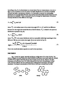
Abstract In this paper, for the first time, the nTFET reliability and stability have been studied against the adverse effect of positive bias temperature instability (PBTI) for three different device architectures, viz. elevated drain-(ED-), elevated source(ES-) and elevated source–drain-(ESD-) TFETs, in terms of threshold voltage (V T ) shift, on-current/off-current (I ON /I OFF ) deviation, off-current (I OFF ) deviation and minimum subthreshold swing (SSmin ) deviation for different PBTI stress conditions. The channel lengths for all the devices have been considered as 70 nm. It is found that the ES-TFET is showing maximum stability against the PBTI effect in terms of I OFF and I ON with a V T shift of 2.9% and SSmin shift of 27%, while maintaining measurable absolute values of the aforementioned device parameters. Keywords Device architecture optimization · Elevated source–drain · PBTI · Interface trap charges · Tunnel FET · TFET reliability
1 Introduction Continuous device miniaturization over the last few decades, in order to fulfill the increasing demand of “All-in-one” or “All-in-palm” concept, the need of devices, fit to work for next generation low-power electronics, has gained a lot of research attention. S. Das (B) Department of Electronics and Communication Engineering, Sikkim Manipal Institute of Technology, Sikkim Manipal University, Sikkim, India e-mail: [email protected] A. Chattopadhyay · S. Tewari Department of Radio Physics and Electronics, University of Calcutta, Kolkata, India e-mail: [email protected] S. Tewari e-mail: [email protected]
© The Editor(s) (if applicable) and The Author(s), under exclusive license to Springer Nature Singapore Pte Ltd. 2021 V. Nath and J. K. Mandal (eds.), Proceedings of the Fourth International Conference on Microelectronics, Computing and Communication Systems, Lecture Notes in Electrical Engineering 673, https://doi.org/10.1007/978-981-15-5546-6_14
159
160
S. Das et al.
In this regard, Tunnel FET (TFET), due to its ability to overcome the 60 mV/decade subthreshold slope (SS) limitation at room temperature, of the conventional MOSFET devices, has emerged as a savior [1–5]. But Tunnel FET suffers from low ION value, which makes it difficult to use the device for analog application. But in order to overcome this shortcoming of the TFET device, alternate high mobility channel materials [6] as well as several novel device architectures have been proposed [7–15]. L-shaped and U-shaped gates [15, 16] are the examples of such innovative device architectures. Here, the vertical tunneling mechanism in addition to horizontal tunneling mechanism has been used, which increases the effective tunneling area, without affecting the device footprint and ultimately leading to an enhanced device current as well as a sharp subthreshold swing. However, in search for strict device performance improvement, the aspect of device stability and reliability against adverse effects, viz. bias temperature instability (BTI), hot carrier stress (HCS), etc., have been overloo
Data Loading...