Optical and Electrical Properties of Undoped Microcrystalline Silicon Deposited by the VHF-GD with Different Dilutions o
- PDF / 483,948 Bytes
- 6 Pages / 414.72 x 648 pts Page_size
- 42 Downloads / 329 Views
761
Mat. Res. Soc. Symp. Proc. Vol. 452 01997 Materials Research Society
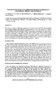
EXPERIMENTAL The samples were deposited by the VHF-GD deposition technique at a plasma excitation frequency of 110 MHz using a gas purifier [6]. Thereby the ratio of silane flow over total gas flow [SiH 4 ]/[SiH 4 + H 2] was varied between 1.25% and 7.5%. The sample deposited at 7.5% dilution is amorphous, all the others are microcrystalline. With deposition rates ranging from less than 0.7 A/s (1.25% dilution) to 3.5 A/s (7.5% dilution) layer thicknesses between 1.6 and 1.9 pgm were obtained. All films were deposited either on uncoated glass (Schott AF 45) or on chromium-coated glass (for Time of Flight). Semitransparent, small size (-2 mm 2 area) chromium top contacts were deposited for TOF samples, coplanar aluminium contacts with a gap of 0.5 mm were used for dark conductivity and CPM measurements. The optical absorption of the materials was determined by Transmission/Reflection spectroscopy, by Constant Photocurrent Method (CPM) and by Photothermal Deflection Spectroscopy (PDS). The transport properties were studied by dark conductivity measurements at temperatures ranging from 25°C to 180'C. Time of Flight (TOF) measurements in both shorttime and post transient mode were performed respecting the guidelines for TOF measurements on gc-Si:H 1o0 presented in [7]. diffraction X-ray 10' on all measurements microcrystalline samples presented here show a 1000 preferential growth in the direction. A medium grain size of around 200 A and columnar shape of the grains has already been found E 0 in the past for other samples produced using similar 125% deposition conditions [1]. -- .. -f ... 2.5% # A
_4
5% & 7.5% A
RESULTS PDS detection
0.1
Opticl proertieJ: Optical properties It has already been shown [3] that the transition from to m icrocrystalline amorphous material is abrupt and typically takes place around 7.5% dilution for the deposition conditions used here. The optical absorption spectra measured on the present series (represented in figure 1) confirms the drastic change of optical absorption with a variation of the dilution ratio. Thereby, three distinct effects can be observed: the
-. •'•°.al1"
0.01
•
---
limit (sample thickness =2gm)
P
[-
tike
Tm-o c-Si
0.001 0.8
".-.. ............. 1
1.2
1.4
1.6
.
.
...
1.8
2
2.2
I.. 2.4
Energy [eV] Fig. I Optical absorption coefficientfor the 110 MHz dilution series determined by PDS, CPM and Transmission / Reflection measurements: the transition from amorphous to microcrystallinesilicon takes place at around 7.5% dilution. Crystalline silicon data [8] is also plotted for comparison. Note the difference between the CPM and PDS spectrafor the 5% sample, discussed in the text.
762
transition from a-Si:H to g.c-Si:H, scattering and the effect of mixed-phase material.
10.3 _1.25%/c First, the main phenomenon 2.5% E observed is of course the transition Eat 5% from non-direct absorption in 0.22 eV 1 -5 75 amorphous material with a Tauc gap 0.. around 1.7 eV to the optical abs
Data Loading...